Semiconductor structure and fabrication method thereof

a technology of semiconductor structure and fabrication method, applied in the direction of semiconductor/solid-state device details, electrical apparatus, semiconductor devices, etc., can solve the problem that the performance of the semiconductor structure may be easily affected

Active Publication Date: 2019-02-05
SEMICON MFG INT (SHANGHAI) CORP +1
View PDF10 Cites 0 Cited by
  • Summary
  • Abstract
  • Description
  • Claims
  • Application Information

AI Technical Summary

Benefits of technology

[0018]The conductive wire may be connected with an external chip across the protective region. Because the top interlayer dielectric may cover the seal ring structure entirely, the portion of the passivation layer in the protective region may have no protruding portion. Thus, the passivation layer may be uneasy to connect with the conductive wire. Thus, the isolation property between the seal ring structure and the conductive wire may be increased. Accordingly, it may be uneasy to form a leakage current in the semiconductor structure; and the performance of the semiconductor structure may be improved.
[0018]The conductive wire may be connected with an external chip across the protective region. Because the top interlayer dielectric may cover the seal ring structure entirely, the portion of the passivation layer in the protective region may have no protruding portion. Thus, the passivation layer may be uneasy to connect with the conductive wire. Thus, the isolation property between the seal ring structure and the conductive wire may be increased. Accordingly, it may be uneasy to form a leakage current in the semiconductor structure; and the performance of the semiconductor structure may be improved.

Problems solved by technology

However, the performance of the semiconductor structure may be easily affected by conventional fabrication methods.

Method used


Image

  • Semiconductor structure and fabrication method thereof
  • Semiconductor structure and fabrication method thereof
  • Semiconductor structure and fabrication method thereof

Examples


Embodiment Construction

[0014]Reference will now be made in detail to exemplary embodiments of the disclosure, which are illustrated in the accompanying drawings. Wherever possible, the same reference numbers will be used throughout the drawings to refer to the same or like parts.

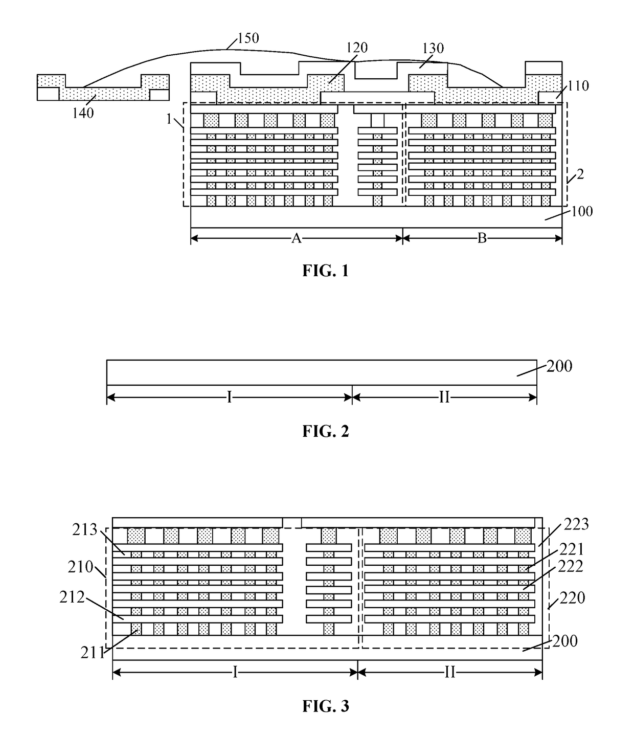
[0015]FIG. 1 illustrates a semiconductor structure. As shown in FIG. 1, the semiconductor structure includes a semiconductor substrate 100. The semiconductor substrate 100 includes a device region “A” and a protective region “B” around the device region “A”. The semiconductor structure also includes a seal ring structure 1 on the semiconductor substrate 100 in the protective region “B”; and device structures (not shown) on the semiconductor substrate 100 in the device region “B”. Further, the semiconductor structure may also include an electrical interconnect structure 2 and an interlayer dielectric layer 110 on the seal ring structure 1 and the electrical interconnect structure 2. The interlayer dielectric layer 110 has an openin...


PUM


Abstract

Semiconductor structures and fabrication methods thereof are provided. An exemplary semiconductor structure includes a semiconductor substrate having a device region and a protective region around the device region; a seal ring structure on the semiconductor substrate in the protective region; an electrical interconnect structure on the semiconductor substrate in the device region; an interlayer dielectric layer entirely covering the protective region on the seal ring structure and the electrical interconnect structure; a solder pad electrically connected with the electrical interconnect structure passing through a portion of the interlayer dielectric layer in the device region; a passivation layer on the interlayer dielectric layer and exposing the solder pad; and a conducive wire connected to the solder pad and across over a portion of the passivation layer in the protective region.

Description

CROSS-REFERENCES TO RELATED APPLICATIONS[0001]This application claims the priority of Chinese patent application No. 201611110242.1, filed on Dec. 2, 2016, the entirety of which is incorporated herein by reference.FIELD OF THE DISCLOSURE[0002]The present disclosure generally relates to the field of semiconductor manufacturing technologies and, more particularly, relates to semiconductor structures and fabrication methods thereof.BACKGROUND[0003]With the continuous development of semiconductor technologies, the sizes of the integrated circuits (ICs) have been continuously reduced; and the performance of the semiconductor device has been continuously improved.[0004]To reduce effect of external environments on the semiconductor devices in a chip, a seal ring structure is often formed around the semiconductor devices in the chip. To allow the seal ring structure to be able to reduce the stress generated by the external environments to the semiconductor devices, the seal ring structure o...

Claims


Application Information

Patent Timeline
Patent Type & Authority Patents(United States)
IPC IPC(8): H01L23/48H01L21/70H01L23/045H01L23/051H01L23/00H01L23/10H01L23/58H01L25/065H01L25/18H01L25/16H01L25/10H01L25/07
CPCH01L23/10H01L21/70H01L23/045H01L23/051H01L23/562H01L23/564H01L23/585H01L25/18H01L24/05H01L25/065H01L25/07H01L25/10H01L25/16H01L21/56H01L23/3171H01L24/03H01L24/07H01L24/08H01L2224/0801H01L2224/081H01L2224/04042H01L2224/48137H01L2224/45147H01L2224/45124H01L24/45H01L2224/02166H01L2224/05647H01L2224/05624H01L24/48H01L2924/14H01L23/3157H01L2924/00014H01L2924/01029
Inventor SONG, CHUNZHONG, YI
Owner SEMICON MFG INT (SHANGHAI) CORP
Why Eureka
Try Eureka