Side-view light emitting laser element

a technology of light-emitting laser elements and side-view, which is applied in the direction of lasers, semiconductor devices, semiconductor lasers, etc., can solve the problems of poor crystal quality, easy cracking, and weakened light confinement ability of cladding layers with overly low thickness, so as to enhance light-emitting performance and product life.

Active Publication Date: 2019-02-19
LEXTAR ELECTRONICS CORP
View PDF4 Cites 3 Cited by
  • Summary
  • Abstract
  • Description
  • Claims
  • Application Information

AI Technical Summary

Benefits of technology

[0005]An aspect of the disclosure is to provide a side-view light emitting laser element for enhancing light emitting performances and product life thereof.
[0007]Thus, compared to the conventional arts in which the thickness of the cladding layers, the traditional semiconductor laser element is needed to be controlled accurately in order to prevent from reducing the light confinement ability of the cladding layers and the cladding layers getting cracked. Therefore, since the electrode (cladding) layers of the side-view light emitting laser element of the embodiment respectively are with better refractive index, not only the light confinement abilities of the side-view light emitting laser element can be increased, but also the side-view light emitting laser element will not be cracked easily.

Problems solved by technology

However, when aluminum gallium nitride (AlGaN) is adopted as the cladding layers in a traditional semiconductor laser element, fragmentations or poor crystal quality of the cladding layers might occur so as to greatly affect yield, quality and product life of the traditional semiconductor laser element.
Otherwise, the light confinement ability of the cladding layers with overly lower thickness may be weakened, or the cladding layers with overly higher thickness may lead to being cracked easily.

Method used


Image

  • Side-view light emitting laser element
  • Side-view light emitting laser element
  • Side-view light emitting laser element

Examples


Embodiment Construction

[0027]Reference will now be made in detail to the present embodiments of the disclosure, examples of which are illustrated in the accompanying drawings. Wherever possible, the same reference numbers are used in the drawings and the description to refer to the same or like parts. According to the embodiments, it will be apparent to those skilled in the art that various modifications and variations can be made to the structure of the present disclosure without departing from the scope or spirit of the disclosure.

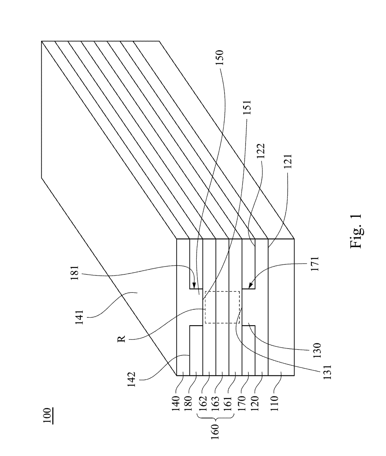
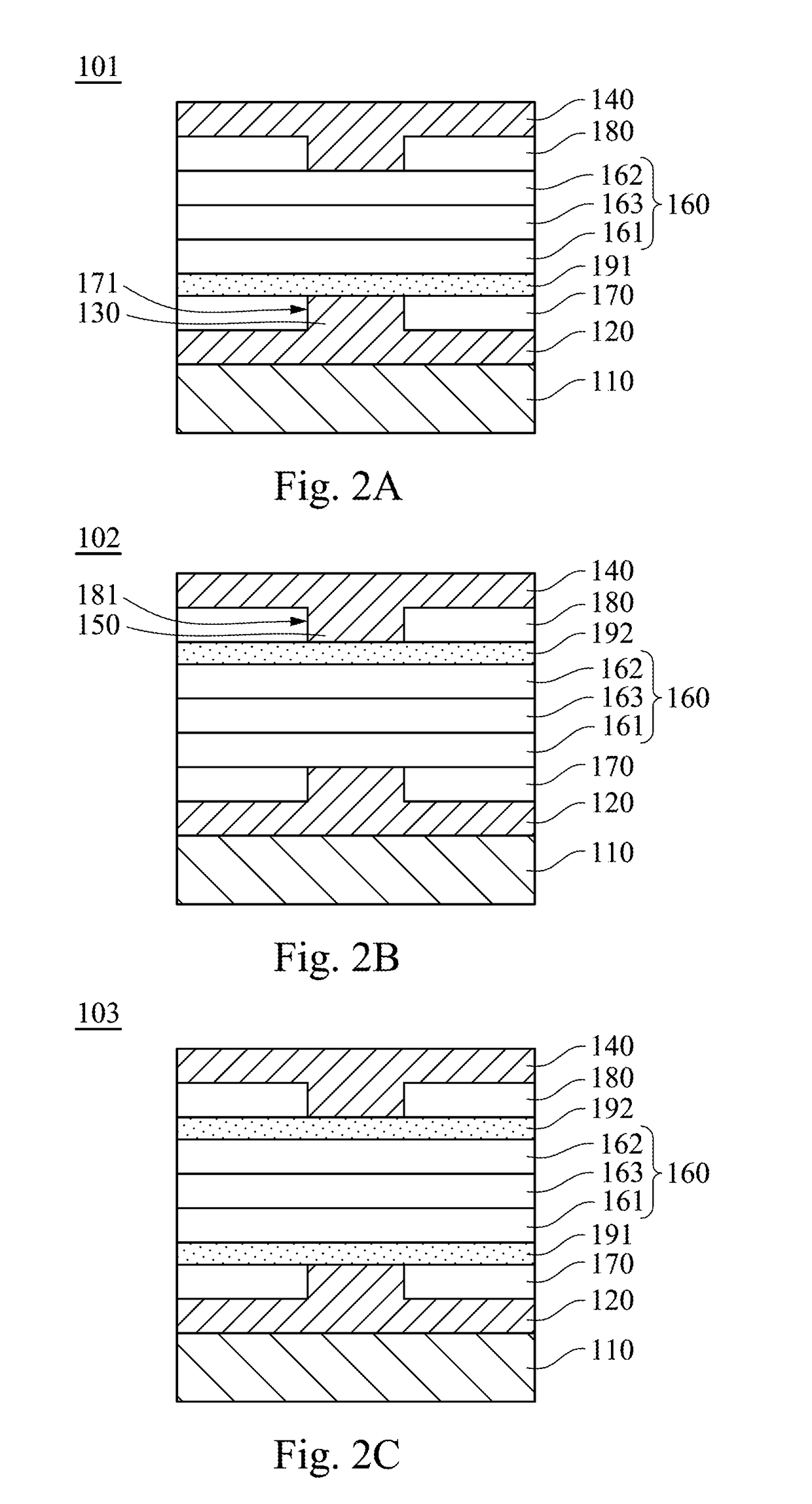
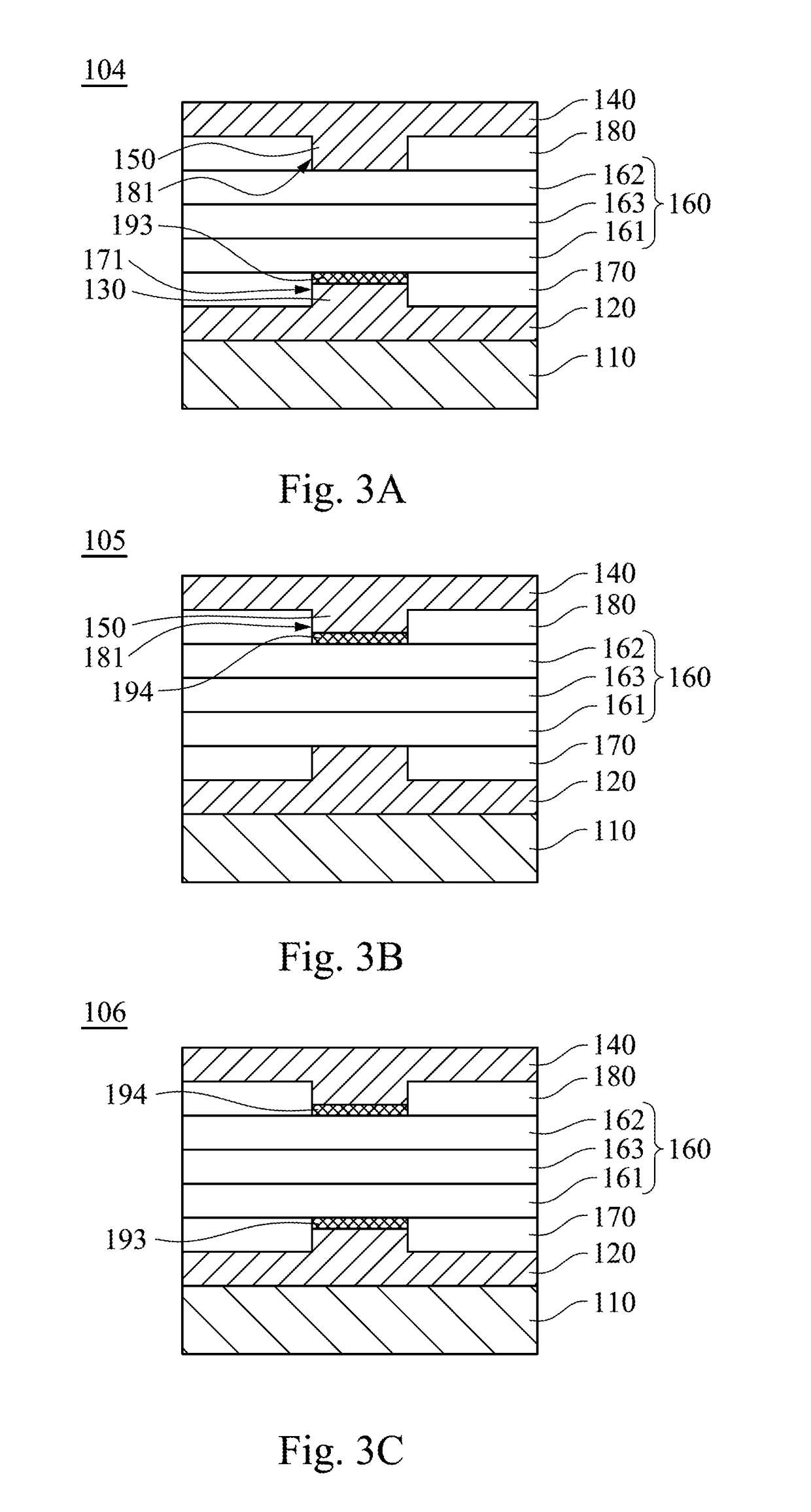
[0028]Reference is now made to FIG. 1 in which FIG. 1 is a three-dimensional sectional view of a side-view light emitting element 100 according to one embodiment of the disclosure. As shown in FIG. 1, in the embodiment, the side-view light emitting element 100 includes a support substrate 110, a first cladding layer 120, a light emitting multilayer unit 160 and a second cladding layer 140. The first cladding layer 120 is disposed on the support substrate 110. The second claddi...


PUM


Abstract

A side-view light emitting laser element includes a support substrate, a first electrode layer, a second electrode layer, and a light emitting multilayer unit sandwiched between the first electrode layer and the second electrode layer. The first electrode layer is disposed on the support substrate. The second electrode layer is disposed on the first electrode layer. The light emitting multilayer unit includes a first semiconductor layer, a second semiconductor layer and an activating layer sandwiched between the first semiconductor layer and the second semiconductor layer. A first refractive index of the first electrode layer and a second refractive index of the second electrode layer are between 1 and 0, respectively.

Description

RELATED APPLICATIONS[0001]This application claims priority to Taiwan Application Serial Number 105121257, filed Jul. 5, 2016, which is herein incorporated by reference.BACKGROUNDField of Disclosure[0002]The present disclosure relates to a light emitting element. More particularly, the present disclosure relates to a side-view light emitting element.Description of Related Art[0003]In general, a semiconductor laser element is able to confine light waves generated by electrons and electron holes with a resonant cavity spaced to form between two cladding layers of a semiconductor laser element. By generating standing wave oscillation to form stimulated emissions and repeatedly enhance to a certain critical point, coherent light with the same phase, polarization and radiation direction can be stimulated.[0004]However, when aluminum gallium nitride (AlGaN) is adopted as the cladding layers in a traditional semiconductor laser element, fragmentations or poor crystal quality of the cladding...

Claims


Application Information

Patent Timeline
Patent Type & Authority Patents(United States)
IPC IPC(8): H01S5/32H01L33/60H01S5/042H01S5/18H01S5/20
CPCH01S5/3211H01L33/60H01S5/20H01S5/18H01S5/0425H01S5/04253H01S5/3214H01S5/2027
Inventor WANG, TE-CHUNGKUO, SHIOU-YICHEN, JUN-RONG
Owner LEXTAR ELECTRONICS CORP
Why Eureka
Try Eureka