

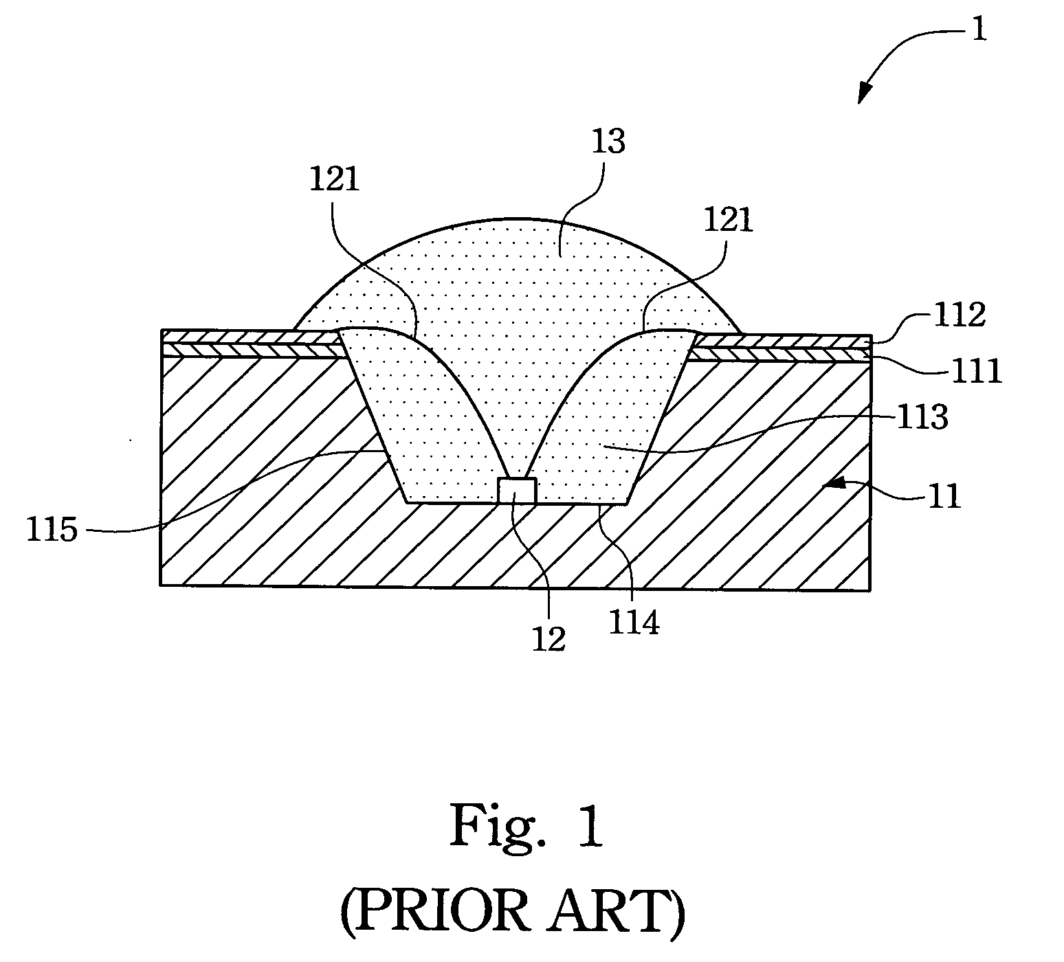
Light emitting diode packaging structure
a technology of light-emitting diodes and packaging structures, which is applied in the direction of basic electric elements, electrical equipment, semiconductor devices, etc., can solve the problems of adversely reducing the brightness of led lights, reducing the light-emitting effect of led lights, and reducing light-emitting losses. , to achieve the effect of enhancing the light-emitting effect of an led, reducing reflection loss, and improving light-emitting flux
- Summary
- Abstract
- Description
- Claims
- Application Information
AI Technical Summary
Benefits of technology
Problems solved by technology
Method used
Image

Examples
Embodiment Construction
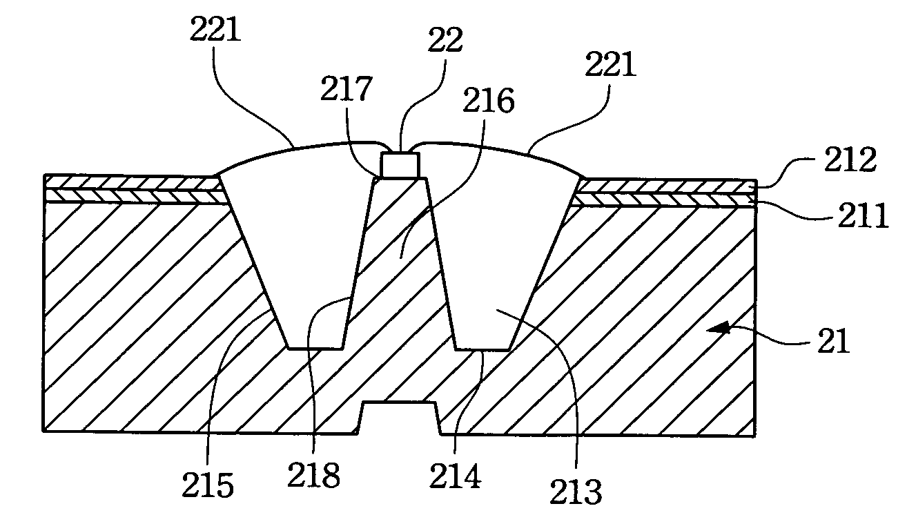
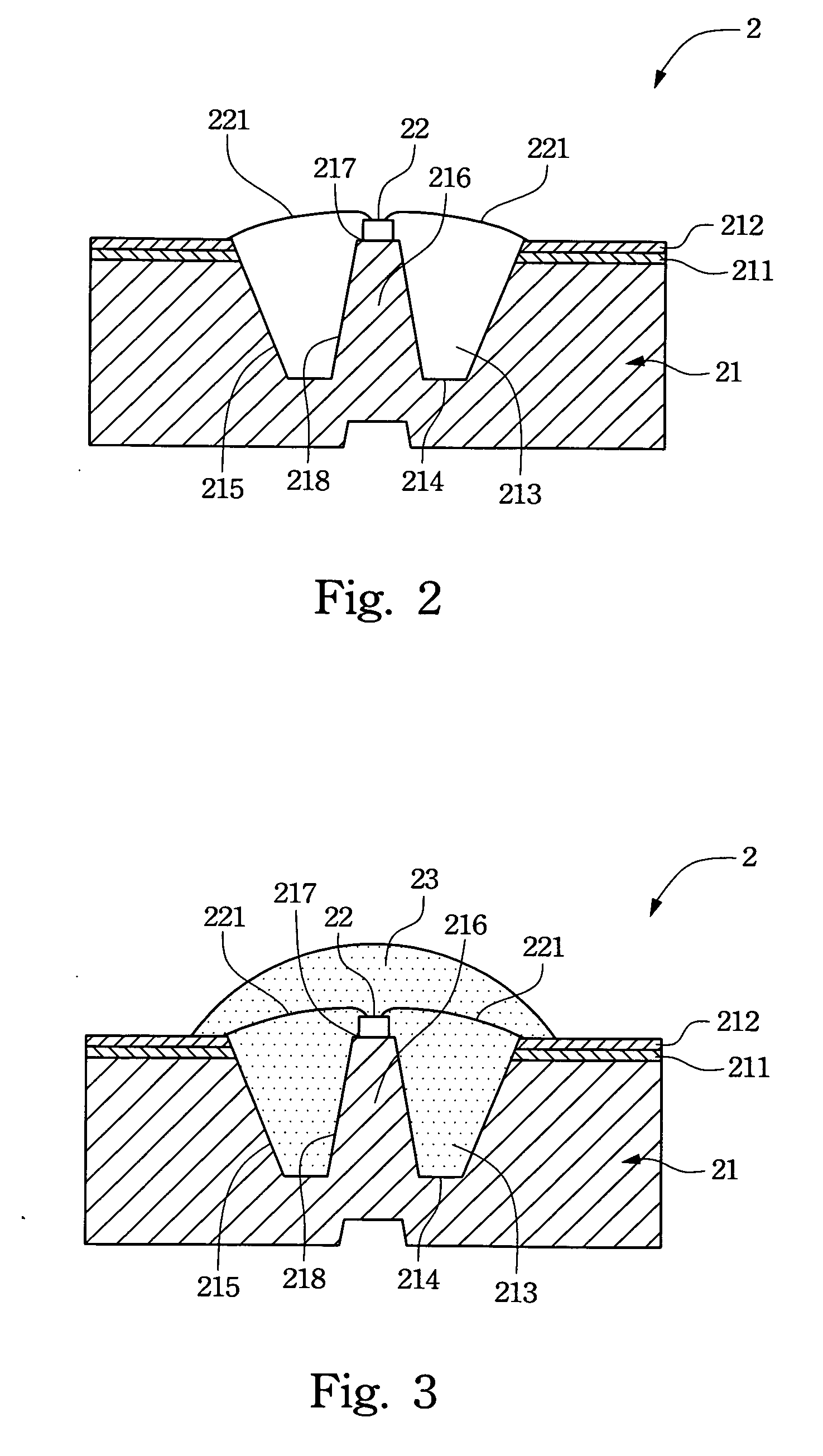
[0016] Reference is made to FIG. 2, a cross-sectional view showing an LED packaging structure 2 according to a first embodiment of the present invention. As shown, the packaging structure 2 includes a carrier 21 and an LED chip 22.
[0017] The carrier 21 is made of a material with high radiating power, such as gold, silver, copper, tungsten, molybdenum, tin, zinc, indium, aluminum, etc., or an alloy thereof. On a top surface of the carrier 21, there is provided an insulating layer 211. A conducting layer 212 consisting of conducting circuits is further provided on the insulating layer 211. The top surface of the carrier 21 is partially depressed to form a cup portion 213 having a raised central seat 216 projected from a bottom 214 thereof. A top surface 217 of the raised central seat 216 is preferably flush with or higher than a top surface of the conducting layer 211.
[0018] The LED chip 22 is mounted on the top surface 217 of the raised central seat 216, and is electrically connect...
PUM
 Abstract
Description
Claims
Application Information