Semiconductor module with two auxiliary emitter conductor paths

a semiconductor and auxiliary technology, applied in the field of high-power semiconductors, can solve the problems of inability to help gate resistors, inability to use gate resistors, and inability to solve gate interference problems,

Active Publication Date: 2019-03-05
HITACHI ENERGY LTD
View PDF13 Cites 0 Cited by
  • Summary
  • Abstract
  • Description
  • Claims
  • Application Information

AI Technical Summary

Benefits of technology

[0012]In case of paralleled IGBTs, due to asymmetric module layouts, each IGBT may see a different UGE causing unbalanced dynamic current sharing. The advantages on the other hand are, as can be seen from above equations, that the effective gate voltage UG′E′ is reduced when dl / dt is increasing, which acts as self-damping in case of high dl / dt thus providing effective built-in short circuit protection.
[0013]The objective of the invention is to provide an easy to control and easy to configure semiconductor module with built-in short-circuit protection.
[0018]Furthermore, the semiconductor module comprises a first conductor path connected to the emitter and a second conductor path connected to the emitter having a different mutually inductive coupling with the emitter conductor path as the first conductor path. It has to be understood that a conductor path may be any type conductor like a metal strip, a wire, or a strip line on a circuit board. The two conductor paths are used for providing different ways of connecting the gate terminal to the emitter. In particular, the different paths have different coupling to the emitter conductor path and therefore, by choosing to connect one or both of the conductor paths to the gate allows to control its switching characteristics using the above described effect.
[0019]According to an embodiment of the invention, the first conductor path and the second conductor path are connectable to the auxiliary emitter terminal. For example, the semiconductor module only has one auxiliary emitter terminal, but provides the possibility to connect the auxiliary emitter terminal via the first, the second or both conductor paths with the emitter. In this way, the semiconductor module may be configured to provide the desired coupling with the main emitter conductor path at one auxiliary emitter terminal.

Problems solved by technology

On the other hand, fast switching may also cause electromagnetic interference problems.
However, gate resistors usually do not help in case of short circuits and intelligent gate drivers may be expensive and complex to implement and control.
Otherwise switching would be too slow.
The PCB design cannot compensate the coupling.
Other types of modules do not provide auxiliary emitter terminals at all, thus leaving the responsibility to the PCB and gate drive designer.
As a rule, short circuit protection for modules with low dl / dt damping has to be applied with external circuits, typically adding extra losses and extra components.

Method used


Image

  • Semiconductor module with two auxiliary emitter conductor paths
  • Semiconductor module with two auxiliary emitter conductor paths
  • Semiconductor module with two auxiliary emitter conductor paths

Examples


Embodiment Construction

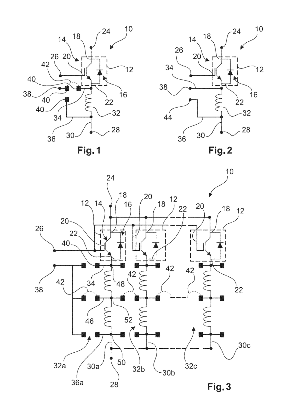
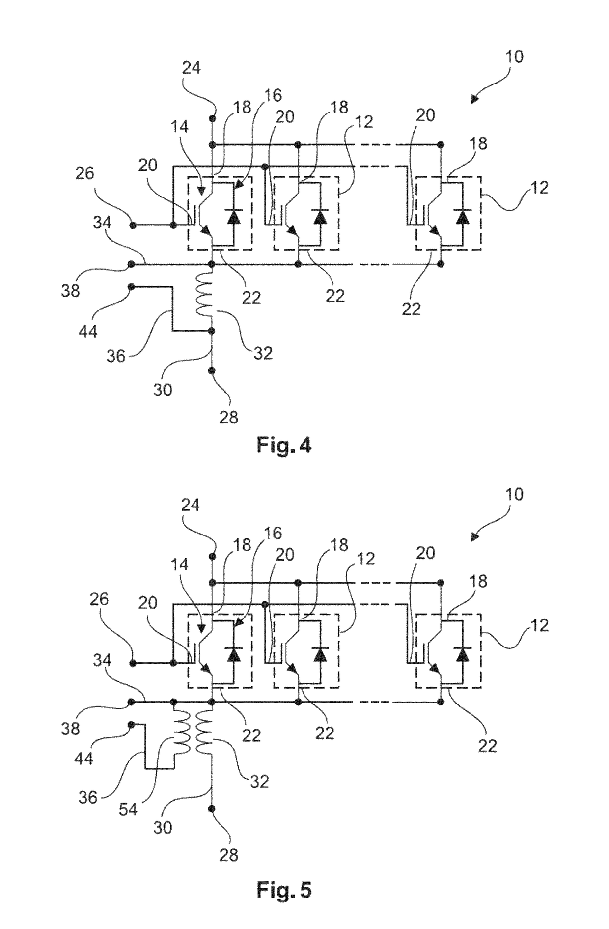
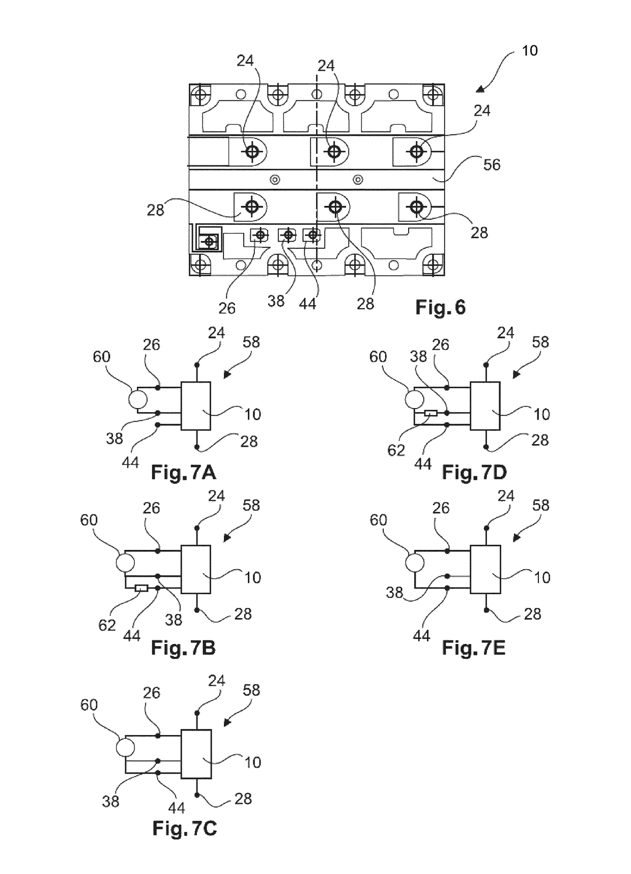
[0008]Fast switching IGBTs generate high dl / dt and dU / dt, which may be the sources of various electromagnetic interference problems inside and outside the semiconductor modules. This electromagnetic interference effect originate from the relations Uind=L*dl / dt and Iind=C*dl / dt.

[0009]One important design parameter inside an IGBT module is the so-called common emitter stray inductance Lσ_CE between the main emitter terminal and the auxiliary emitter terminal used to connect the gate-emitter voltage to turn the device on and off. Considering the typically high turn-on / off collector currents (dlc / dt), the voltage drop across that common emitter stray inductance Lσ_CE may become significant. Because of the induced voltage, the IGBT chip sees a different effective gate voltage UG′E′ than the gate voltage applied at the module terminals UGE.

[0010]The following formulas describe the relation between the induced UGE voltage across the common emitter stray inductance Lσ_CE and the effective g...


PUM


Abstract

A semiconductor module comprises a semiconductor chip comprising a semiconductor switch having a collector, emitter and gate, a collector terminal connected to the collector, gate terminal connected to the gate, an emitter terminal connected to the emitter via an emitter conductor path having an emitter inductance, an auxiliary emitter terminal connected to the emitter, a first conductor path connected to the emitter, and a second conductor path connected to the emitter having a different mutually inductive coupling with the emitter conductor path as the first conductor path. The first conductor path and the second conductor path are connectable to the auxiliary emitter terminal and / or the first conductor path is connected to the auxiliary emitter terminal and the second conductor path is connected to a second auxiliary emitter terminal. The semiconductor switch is an IGBT and each of the first conductor path and the second conductor path comprises bridging points for connecting the respective conductor path to the auxiliary emitter terminal.

Description

FIELD OF THE INVENTION[0001]The invention relates to the field of high power semiconductor. In particular, the invention relates to a semiconductor module and a semiconductor assembly.BACKGROUND OF THE INVENTION[0002]Semiconductor modules comprise one or more semiconductor chips, which each comprise one or more semiconductors like diodes, transistors, thyristors and the like. In such modules, high power semiconductor switches like IGBTs are used for switching currents of more than 10 A and / or more than 1000 V.[0003]As a rule, switching losses should be kept at a minimum, which may be achieved by fast switching. On the other hand, fast switching may also cause electromagnetic interference problems. The switching speed is therefore often controlled via a gate resistor or via intelligent gate drives controlling the gate current IC (for example by using IC or dlc / dt feedback). However, gate resistors usually do not help in case of short circuits and intelligent gate drivers may be expen...

Claims


Application Information

Patent Timeline
Patent Type & Authority Patents(United States)
IPC IPC(8): H01L29/739H01L29/417H01L27/088H03K17/081H01L29/423H01L23/00H01L23/02H03K17/12H01L25/07H01L23/64H02M1/088H03K17/0424H03K17/082
CPCH01L29/7393H01L23/02H01L23/645H01L24/48H01L25/072H01L27/088H01L29/41708H01L29/4232H03K17/08116H03K17/127H03K17/0828H01L2224/4813H01L2924/0002H01L2924/13055H02M1/088H03K17/0424H01L2924/00H01L2924/00014H01L2224/45099H01L2224/85399H01L2224/05599
Inventor HARTMANN, SAMUELCOTTET, DIDIERKICIN, SLAVO
Owner HITACHI ENERGY LTD
Why Eureka
Try Eureka