Method and apparatus for generating input images for holographic waveguide displays

a technology of input image and waveguide, applied in the direction of optics, instruments, optical light guides, etc., can solve the problems of reducing diffraction efficiency, unable to apply sufficient voltage, and exhibiting near 100% efficiency of the device with no voltage applied, so as to achieve low chromatic dispersion, efficient coupling, and high efficiency

Active Publication Date: 2019-03-26
DIGILENS
View PDF1484 Cites 53 Cited by
  • Summary
  • Abstract
  • Description
  • Claims
  • Application Information

AI Technical Summary

Benefits of technology

[0009]It is a first object of the invention to provide an image generator for illuminating a microdisplay, collimating the reflected image light from the microdisplay and efficiently coupling it into a thin holographic waveguide with high efficiency, with low chromatic dispersion and with high illumination uniformity.
[0010]It is a second object of the invention to provide a waveguide display comprising an image generator for illuminating a microdisplay, collimating the reflected image light from the microdisplay and efficiently coupling it into a thin holographic waveguide with high efficiency, with low chromatic dispersion and with high illumination uniformity, and holographic waveguides for providing pupil expansion in orthogonal directions.

Problems solved by technology

The device exhibits near 100% efficiency with no voltage applied and essentially zero efficiency with a sufficiently high voltage applied.
Reducing the thickness of the grating leads to a decrease in the diffraction efficiency and a broadening of the diffraction efficiency angular bandwidth.
A major design challenge is coupling the image content into the waveguide efficiently and in such a way the waveguide image is free from chromatic dispersion and brightness non uniformity.
However, lasers and other narrow band sources such as LEDs suffer from the problem of pupil banding artifacts which manifest themselves as output illumination non uniformity.

Method used


Image

  • Method and apparatus for generating input images for holographic waveguide displays
  • Method and apparatus for generating input images for holographic waveguide displays
  • Method and apparatus for generating input images for holographic waveguide displays

Examples


Embodiment Construction

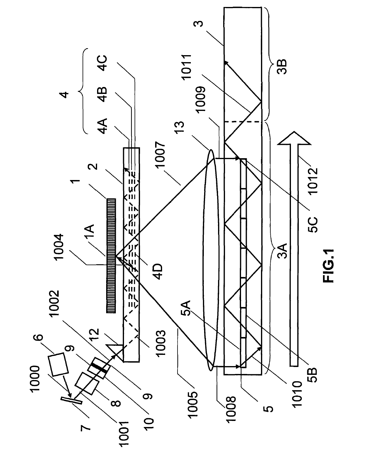
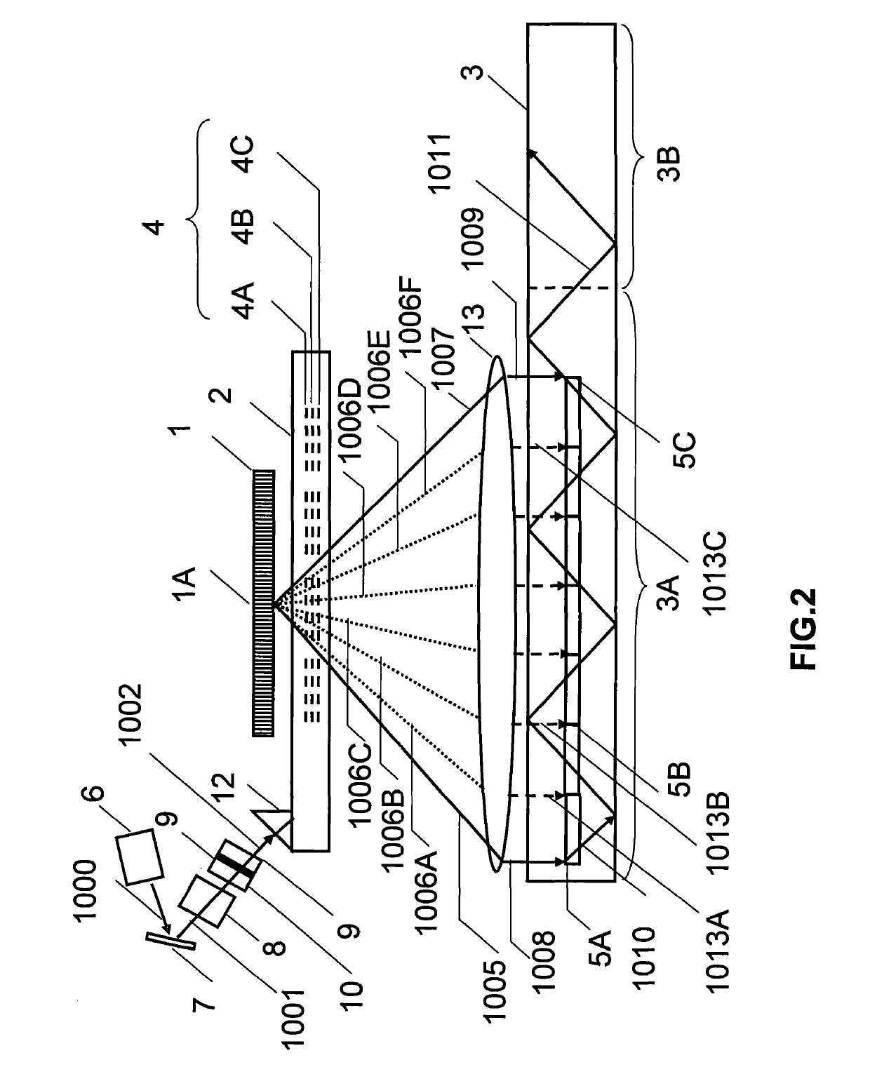
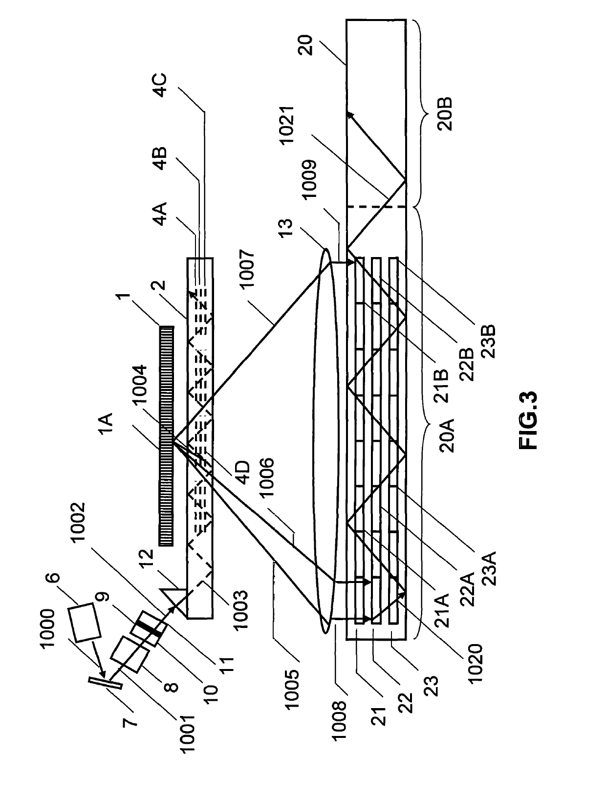
[0048]The invention will now be further described by way of example only with reference to the accompanying drawings. It will apparent to those skilled in the art that the present invention may be practiced with some or all of the present invention as disclosed in the following description. For the purposes of explaining the invention well-known features of optical technology known to those skilled in the art of optical design and visual displays have been omitted or simplified in order not to obscure the basic principles of the invention. Unless otherwise stated the term “on-axis” in relation to a ray or a beam direction refers to propagation parallel to an axis normal to the surfaces of the optical components described in relation to the invention. In the following description the terms light, ray, beam and direction may be used interchangeably and in association with each other to indicate the direction of propagation of light energy along rectilinear trajectories. Parts of the f...


PUM

PropertyMeasurementUnit
thicknessaaaaaaaaaa
total internal reflectionaaaaaaaaaa
wavelengthaaaaaaaaaa

Abstract

An image generation device having: a spatial light modulator; a source of light; a beam deflector; an illumination waveguide and an image transport waveguide, each waveguide containing at least one switchable grating; and a coupler for directing scanned light into a first set of TIR paths in said illumination waveguide. A switchable grating in the illumination waveguide diffracts light onto the SLM, a switchable grating in the image transport waveguide diffracting image-modulated from the SLM into a waveguide path.

Description

CROSS-REFERENCE TO PRIORITY APPLICATION[0001]This application is the U.S. national phase of PCT Application No. PCT / GB2015 / 000203 filed on Jun. 29, 2015, which claims the benefit of U.S. Provisional Patent Application No. 62 / 071,277 filed on Sep. 19, 2014, the disclosures of which are incorporated herein by reference in their entireties.BACKGROUND OF THE INVENTION[0002]This invention relates to an apparatus for generating an image, and more particularly to an apparatus for generating an input image for a holographic waveguide display.[0003]The invention addresses the problem of providing uniform output illumination in holographic waveguide displays. U.S. patent application Ser. No. 13 / 844,456 entitled TRANSPARENT WAVEGUIDE DISPLAY, PCT Application No.: GB2012 / 000677 entitled WEARABLE DATA DISPLAY, U.S. patent application Ser. No. 13 / 317,468 entitled COMPACT EDGE ILLUMINATED EYEGLASS DISPLAY, U.S. patent application Ser. No. 13 / 869,866 entitled HOLOGRAPHIC WIDE ANGLE DISPLAY, and U.S...

Claims


Application Information

Patent Timeline
Patent Type & Authority Patents(United States)
IPC IPC(8): G03H1/00F21V8/00G02B27/42G02F1/29G02B27/01
CPCG02B27/0103G02B6/0035G02B27/01G02B27/017G02B27/425G02F1/29G02B27/4205G02B2027/0174G02B2027/0118G02B2027/0165
Inventor POPOVICH, MILAN MOMCILOWALDERN, JONATHAN DAVIDGRANT, ALASTAIR JOHN
Owner DIGILENS
Why Eureka
Try Eureka