Semiconductor structure and manufacturing method thereof and terminal area structure of semiconductor device

a semiconductor device and semiconductor technology, applied in the direction of semiconductor devices, semiconductor/solid-state device details, electrical apparatus, etc., can solve the problems of reduced breakdown voltage and readily generated leakage current, and achieve the effect of preventing the generation of leakage current and high breakdown voltag

Active Publication Date: 2019-03-26
UPI SEMICON CORP
View PDF6 Cites 0 Cited by
  • Summary
  • Abstract
  • Description
  • Claims
  • Application Information

AI Technical Summary

Benefits of technology

[0005]The invention provides a semiconductor structure and a manufacturing method thereof and a terminal area structure of a semiconductor device that can prevent the generation of leakage current while maintaining a high breakdown voltage.
[0027]Based on the above, in the semiconductor structure and the manufacturing method thereof and the terminal area structure of a semiconductor device provided by the invention, the second conductive layer filled in the first opening can be positioned via the positioning part, and the second conductive layer can be isolated from the substrate via the spacers on the sidewalls of the first opening located at the positioning part, such that the second conductive layer and the first conductive layer can be connected in an effective manner, and the generation of leakage current can be effectively prevented. Via such a structure, the second conductive layer and the first conductive layer can be effectively connected, and therefore a first trench having a larger aperture does not need to be formed, and as a result a shallower first trench having a smaller aperture can be formed to prevent a reduction in breakdown voltage. Moreover, the process complexity of the semiconductor structure and the manufacturing method thereof and the terminal area structure of a semiconductor device provided by the invention is low.

Problems solved by technology

However, the distance between the electrode in a deep trench and the substrate is smaller, such that breakdown voltage is reduced, and leakage current is readily generated.

Method used


Image

  • Semiconductor structure and manufacturing method thereof and terminal area structure of semiconductor device
  • Semiconductor structure and manufacturing method thereof and terminal area structure of semiconductor device
  • Semiconductor structure and manufacturing method thereof and terminal area structure of semiconductor device

Examples


Embodiment Construction

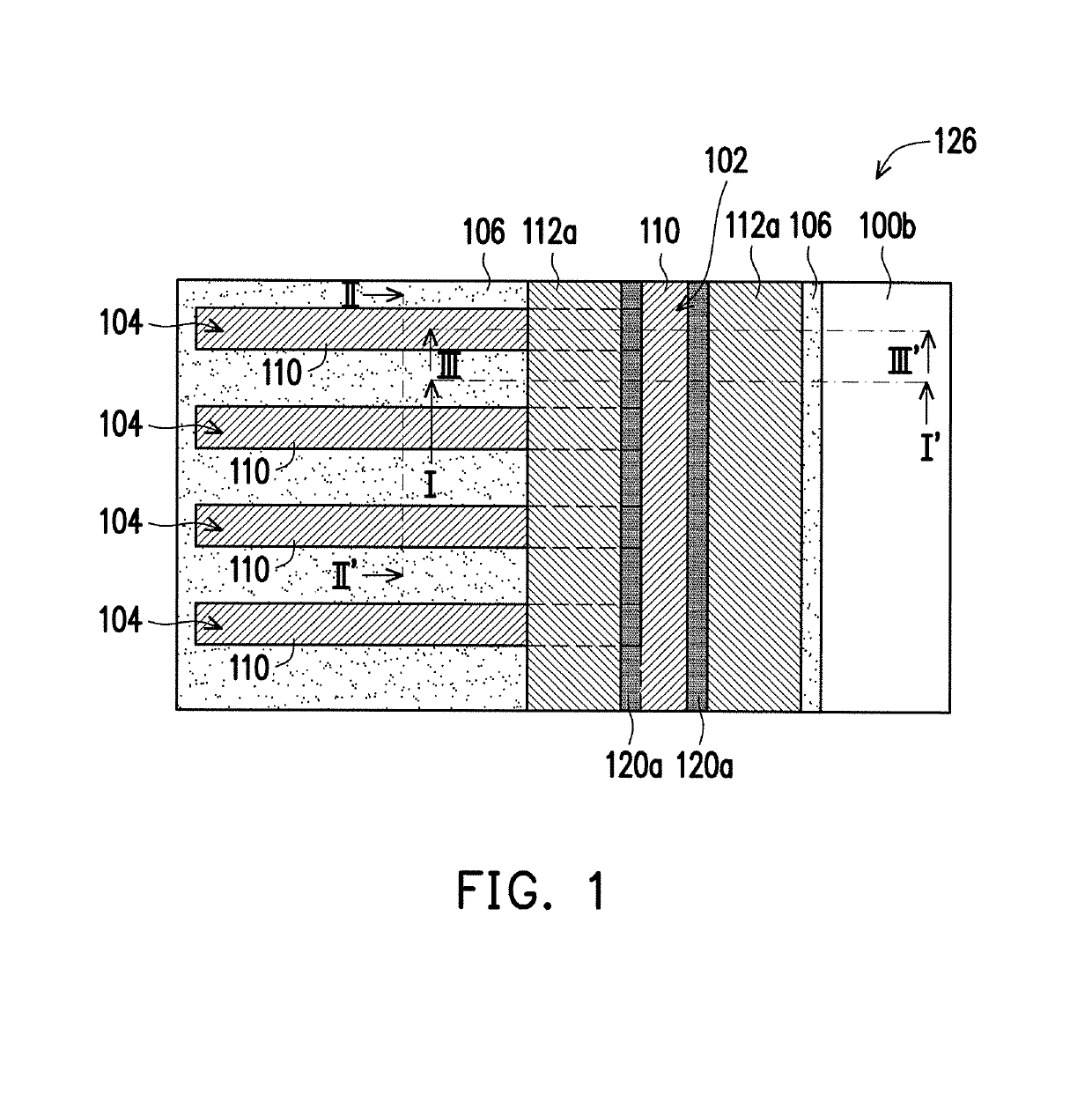
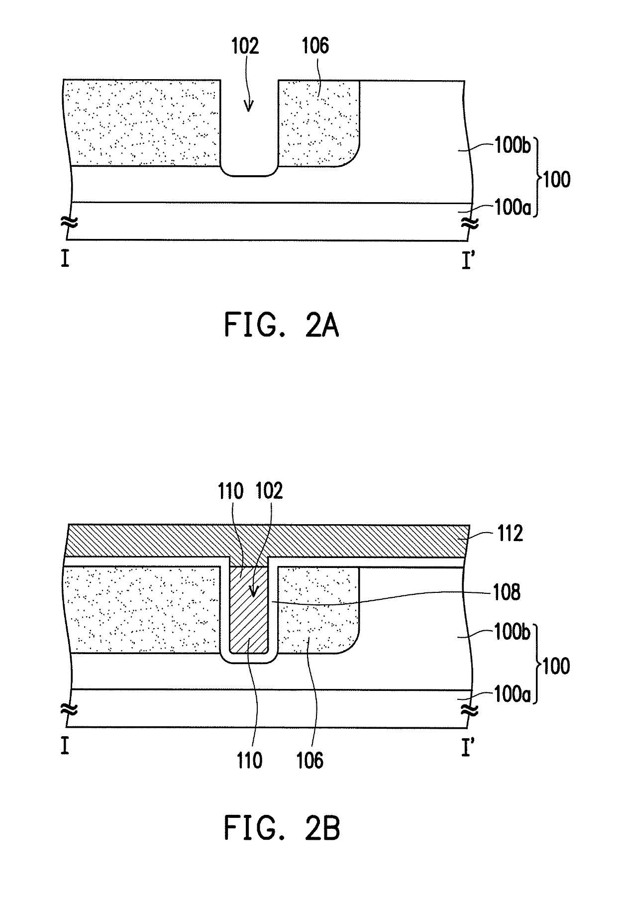
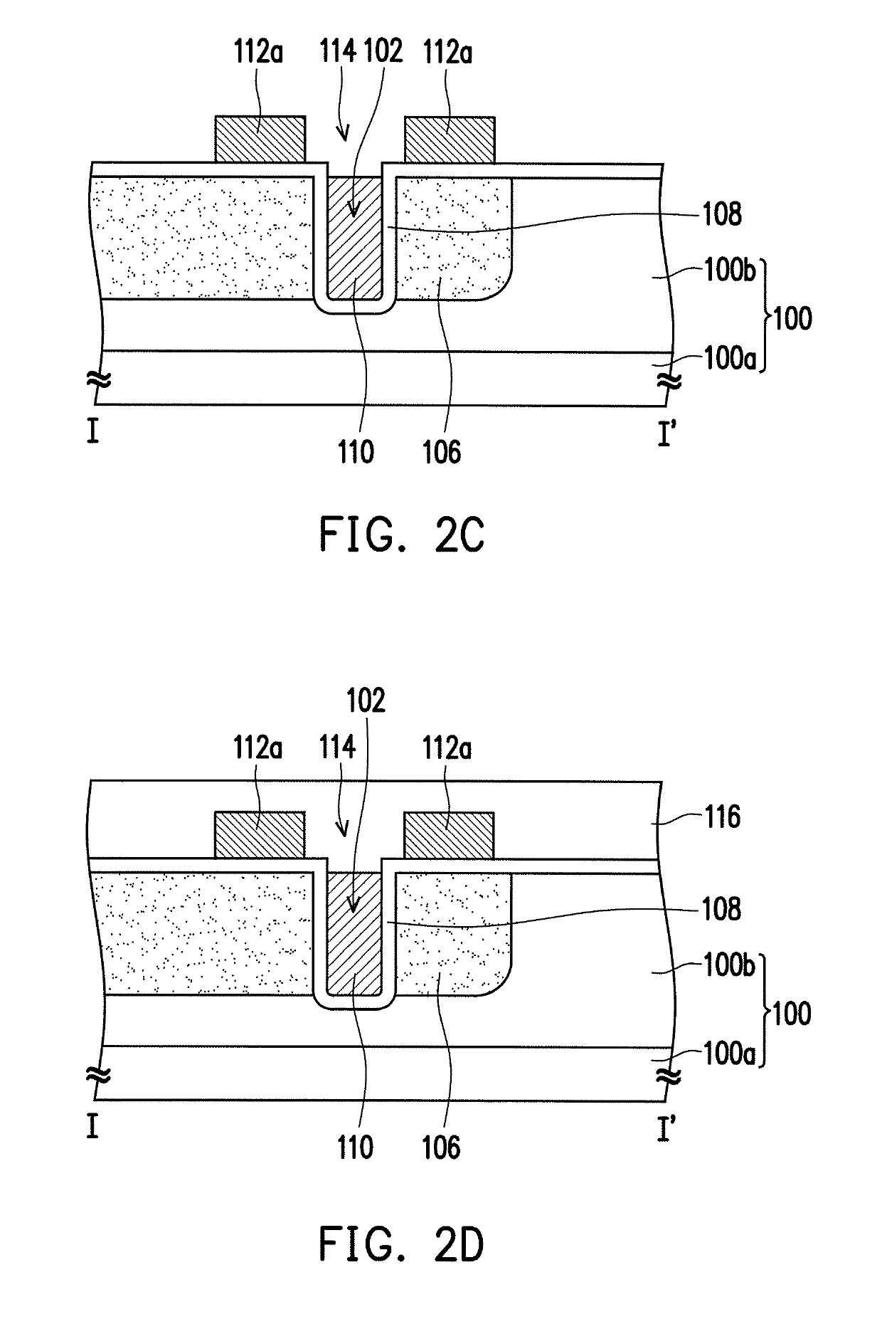
[0034]FIG. 1 is a top view of a semiconductor structure of an embodiment of the invention. For clarity of illustration, FIG. 1 omits some of the components in FIG. 2I and FIG. 3I. FIG. 2A to FIG. 2I are cross sections of the manufacturing process of the semiconductor structure in FIG. 1 along section line I-I′. FIG. 3A to FIG. 3I are cross sections of the manufacturing process of the semiconductor structure in FIG. 1 along section line II-II′. FIG. 4 is a cross section of the semiconductor structure in FIG. 1 along section line III-III′.

[0035]Referring to all of FIG. 1, FIG. 2A, and FIG. 3A, a substrate 100 is provided, and the substrate 100 has a first trench 102. Moreover, the substrate 100 can further have second trenches 104, and the first trench 102 is intersected with the second trenches 104. The second trenches 104 can be parallel to one another. The first trench 102 and the second trenches 104 can be formed at the same time by performing a patterning process on the substrate...


PUM


Abstract

A semiconductor structure including a substrate, a first dielectric layer, a first conductive layer, a positioning part, two spacers, and a second conductive layer is provided. The substrate has a first trench. The first dielectric layer is disposed on a surface of the first trench. The first conductive layer is filled in the first trench and located on the first dielectric layer. The positioning part is disposed on the substrate and has a first opening. The first opening exposes the first trench. The spacers are disposed on two sidewalls of the first opening and expose the first conductive layer. The second conductive layer is filled in the first opening and electrically connected to the first conductive layer. The semiconductor structure can prevent the generation of leakage current while maintaining a high breakdown voltage.

Description

CROSS-REFERENCE TO RELATED APPLICATION[0001]This application claims the priority benefit of Taiwan application serial no. 106116564, filed on May 19, 2017. The entirety of the above-mentioned patent application is hereby incorporated by reference herein and made a part of this specification.BACKGROUND OF THE INVENTIONField of the Invention[0002]The invention relates to a semiconductor structure and a manufacturing method thereof, and more particularly, to a semiconductor structure that can increase breakdown voltage and a manufacturing method thereof and a terminal area structure of a semiconductor device.Description of Related Art[0003]In the interconnect process of a semiconductor structure, when a contact is formed on a wire (such as a gate bus), a trench for forming the wire needs a larger opening to ensure the contact and the wire can be connected in an effective manner.[0004]During the etching process of the trench, a larger opening results in a deeper trench. However, the dis...

Claims


Application Information

Patent Timeline
Patent Type & Authority Patents(United States)
IPC IPC(8): H01L29/66H01L29/40H01L29/423H01L29/76H01L29/94H01L29/06H01L29/78
CPCH01L29/0611H01L29/7813H01L29/66734H01L29/4236H01L23/528H01L29/0615
Inventor TSAI, YI-YUNCHEN, CHIH-HUNGCHEN, CHIN-FU
Owner UPI SEMICON CORP
Why Eureka
Try Eureka