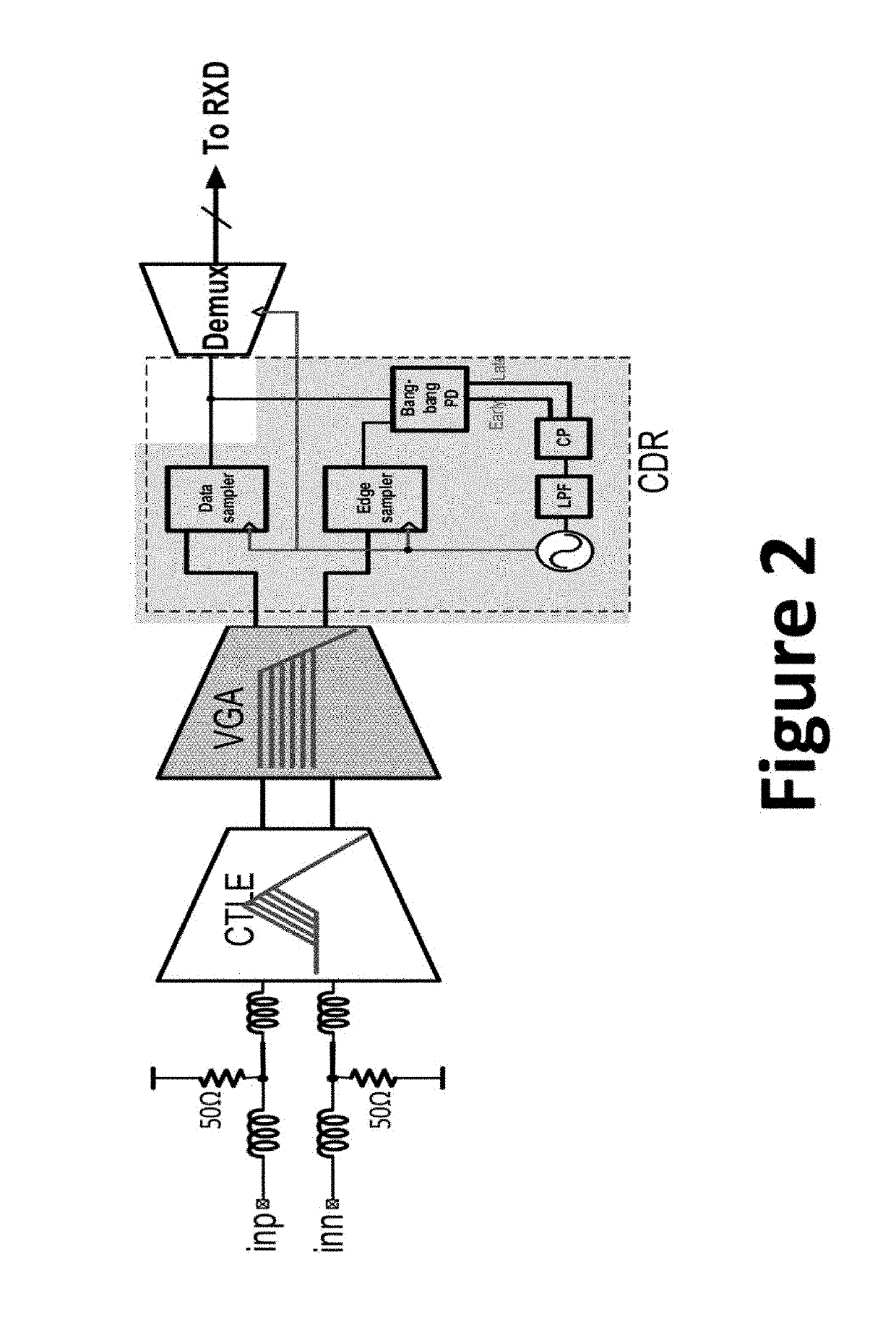
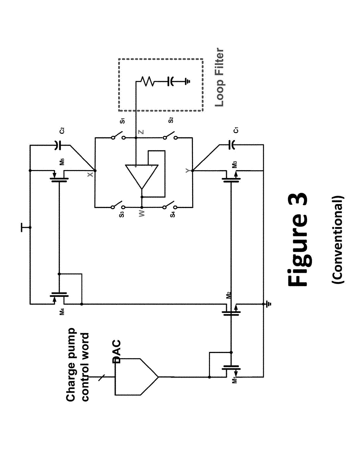
[0022]The present invention is directed to electrical circuits. More specifically, embodiments of the present invention provide a charge pump, which can be utilized as a part of a clock data recovery device. Early and late signals are used as differential input control signals in the charge pump. A first switch and a second switch are used for controlling the direction of the charge pump current. The output voltage of the first switch and the second switch is used in conjunction with a resistor to generate a charge pump current. There are other embodiments as well.
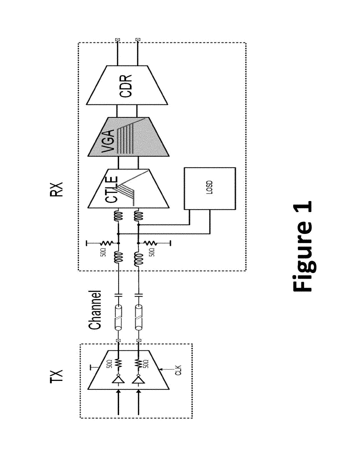
[0023]FIG. 1 is a simplified block diagram illustrating a communication system according to embodiments of the present invention. This diagram is merely an example, which should not unduly limit the scope of the claims. One of ordinary skill in the art would recognize many variations, alternatives, and modifications. In FIG. 1, the transmitter (TX) transits data signal, as a differential signal, to the receiver (RX) via a pair of communication channels. For example, the transmitter and the receiver are implemented as parts of for SerDes systems. At the receiver, the input signals are received at the input terminals with inductive coils and termination resistors that improves the signal integrity. The CTLE module is implemented as a part of the receiver. Input signals are equalized by the CTLE before further processing. For example, loss of signal detection (LOSD) module determines whether there is signal being received. Once it is determined that there are signal coming from the transmitting entity (TX), equalization is performed by the CTLE module. On the other hand, if the LOSD module fails to detect signal presence (or detecting a week signal), signal processing is not performed. For example, the CTLE module is used as a component of an analog front end portion of the communication device. The equalized signal, which is a differential pair, is then provided to the VGA as show. The VGA is specifically configured to amplify the received signal by a predetermined amount, and the VGA operates in conjunction with CLTE. It is to be appreciated that the use of CTLEs with VGAs takes advantage of the fact that CTLEs are essential front end circuit of the receiver devices. For example, receivers are generally implemented with CTLEs followed by one or more VGAs. For example, the VGA is configured to enable constant output voltage swing at the output for a different set of input signal swings by adjusting the gain control code.
[0024]As shown in FIG. 1, after equalization is performed by the CTLE module and adjusted by the VGA, signal processing such as clock data recovery (CDR), analog to digital conversion (ADC), and/or other processes are then performed. The CDR module is configured to determine a frequency for the incoming data and to phase-align the clock to the transition in the data stream. According to embodiments of the present invention, CDR modules include phase detectors that generate early/late signals, and based on the early/late signals, charge pumps inject control amounts of charge into a loop filter. It is to be appreciated that the receiver illustrated in FIG. 1 can be used in a variety of applications and systems. For example, the receiver can be a part of a transceiver device.
[0025]The following description is presented to enable one of ordinary skill in the art to make and use the invention and to incorporate it in the context of the particular applications. Various modifications, as well as a variety of uses in different applications will be readily apparent to those skilled in the art, and the general principles defined herein may be applied to a wide range of embodiments. Thus, the present invention is not intended to be limited to the embodiments presented, but is to be accorded the widest scope consistent with the principles and novel features disclosed herein.
[0026]In the following detailed description, numerous specific details are set forth in order to provide a more thorough understanding of the present invention. However, it will be apparent to one skilled in the art that the present invention may be practiced without necessarily being limited to these specific details. In other instances, well-known structures and devices are shown in block diagram form, rather than in detail, in order to avoid obscuring the present invention.
[0027]The reader's attention is directed to all papers and documents which are filed concurrently with this specification and which are open to public inspection with this specification, and the contents of all such papers and documents are incorporated herein by reference. All the features disclosed in this specification, (including any accompanying claims, abstract, and drawings) may be replaced by alternative features serving the same, equivalent or similar purpose, unless expressly stated otherwise. Thus, unless expressly stated otherwise, each feature disclosed is one example only of a generic series of equivalent or similar features.
[0028]Furthermore, any element in a claim that does not explicitly state “means for” performing a specified function, or “step for” performing a specific function, is not to be interpreted as a “means” or “step” clause as specified in 35 U.S.C. Section 112, Paragraph 6. In particular, the use of “step of” or “act of” in the Claims herein is not intended to invoke the provisions of 35 U.S.C. 112, Paragraph 6.
[0029]Please note, if used, the labels left, right, front, back, top, bottom, forward, reverse, clockwise and counter clockwise have been used for convenience purposes only and are not intended to imply any particular fixed direction. Instead, they are used to reflect relative locations and/or directions between various portions of an object.
[0030]FIG. 2 is a simplified diagram illustrating a receiver apparatus according to embodiments of the present invention. This diagram is merely an example, which should not unduly limit the scope of the claims. One of ordinary skill in the art would recognize many variations, alternatives, and modifications. As shown in FIG. 2, the CDR module is configured between the variable gain amplifier and the de-multiplexer module. More specifically, the CDR module includes a data sampler and an edge sampler. Together, the data sampler and the edge sampler approximate the phase of the clock with respect to the data. In various embodiments, the data sampler and the edge sampler are implemented using sense-amplifier based regeneration flip-flops. Based on the output from the data sampler and the edge sampler, the bang-bang phase detector (and/or other types of phase detector) generates early/late signal, which is used for phase correction. The charge pump (CP) uses the early/late signal from the phase detector (PD) to generate and inject a controlled amount of charge into the loop filter (LPF), and the filtered signal is used to drive the VCO to the correct frequency and phase, the clock output from the VCO given to the data sampler and the edge sampler to provide phase correction. Additionally, the generated clock is provided to the de-multiplexer module as shown. It is important for the charge pump to generate the correct amount of charge for the purpose of phase correction. More specifically, the amount of charge should be the same in early/late phase. Mismatch or incorrect amount of charge would create undesirable phase offset between the clock edge and center of the data eye. As the Bang-Bang phase detector switches from early to late or late to early, the charge pump would introduce charge glitches. For good performance, it is desirable to minimize charge glitches relative to the actual charge generated by the charge pump. For example, charge glitches can be reducing by decreasing the parasitic capacitance on critical nodes.
[0031]FIG. 3 is a diagram illustrating a conventional charge pump architecture for clock and data recovery (CDR). The input signal for early/late indication is receive as a charge pump control word from the digital-to-analog converter (DAC). When late signal is high, switch S1 and switch S4 are closed and charge pump current (i.e., current from transistor M5) is fed into the loop filter and charges the loop filter. When early signal is high switch S2 and switch S3 are turned on and charge pump current (i.e., current form transistor M3) flow away from the loop filter and discharges the loop filter. The operation amplifier configured between the switches reduces the charge sharing between the node Z and W during current switching.
[0032]There are various drawbacks associated with conventional charge pump architecture illustrated in FIG. 3. Transistor M5 and transistor M3 are a matched pair, and their sizes depend on the mismatch requirement between currents. Generally, transistors M5 and M3 are bulky, and hence undesirable parasitic effect associated with nodes X and Y (i.e., respectively corresponding to capacitors C1 and C2) can be significant. During early/late switching, glitch current resulting from charging/discharging capacitors C1 and C2 can be high, and hence this architecture is not suitable for implementations such as low current charge pump. Additionally, charge pump noise depends on the transconductance of transistors M5 and M3, which may contribute to a significant portion of the overall CDR noise. A low noise architecture possible by relaying partially on noise less resisters and transistor currents. It is thus to be appreciated that in various embodiments, the present invention provides novel charge pump implementation used in CDR devices.
[0033]FIG. 4 is simplified diagram illustrating a switching mechanism used in exemplary charge pump implementations according to embodiments of the present invention. This diagram is merely an example, which should not unduly limit the scope of the claims. One of ordinary skill in the art would recognize many variations, alternatives, and modifications. As shown in FIG. 4, differential voltages used in a charge pump are controlled by two switches. In contrast to the architecture illustrated in FIG. 3, which operates in a current mode, the switching mechanism (part of an exemplary charge pump described below) operates in a voltage mode. The inputs Vcp+del and Vcp−del are differential voltages respectively provided to switches S1 and S2. Resistor R is used to convert the differential voltages to currents. It is to be appreciated that the differential voltages, as provided to switches S1 and S2, are characterized by a low impedance, and the charging and discharging currents are generated using the resistor as shown. Switches S1 and S2 are respectively controlled by late and early signals. More specifically, the switch S1 is controlled by a late signal. When switch S1 is on, the current through the resister R would be
[0034] V cp + Del R ,
and this current charges the loop filter. The switch S2 is controlled by the early signal. When it is on, the current through the resister R will be
[0035] V cp - Del R ,
and this current dis-charges the loop filter.
[0036]FIG. 5 is a simplified diagram illustrating a charge pump architecture according to embodiments of the present invention. This diagram is merely an example, which should not unduly limit the scope of the claims. One of ordinary skill in the art would recognize many variations, alternatives, and modifications. As shown in FIG. 5, charge pump control word (or control signal) is received from the DAC. For example, the phase detector generates early and late signals based on the phase obtained from the data sampler and the edge sampler, and the early/late signals are provided as control word generated by the DAC.
[0037]The charge pump control word is controlling the current given by the DAC, and processed by transistors M1 and M2. For example, transistors M1 and M2 as shown are implemented using NMOS transistors, but it is to be understood that other types of transistors can be used as well. The control signal propagates through transistors M3 and M4. As an example, transistors M3 and M4 can be implemented using NMOS transistors as shown, but it is to be understood that other types of transistors can be used as well. Transistor M4 generates a reference current ICP. The operational amplifier OA1 adjusts the gate voltage of transistor M5 until transistor M5 current equals to the current at transistor M4, and voltage at node Y equals to loop filter voltage Vcp. As explained above, voltage input to the switches S1 and S2 are differential voltages. That is, voltages at node X and node Z are pure differential around the common mode voltage of the loop filter. Voltage at node X is Vx=Vcp+Icp*R1. Voltage at node Z is Vz=Vcp−Icp*R1. The low pass filter formed by resistor Rc and capacitor Cc generates stable voltage reference at node xf,zf. For example, resistor Rc and capacitor Cc directly coupled to node Xf form a low-pass resistor for switch S1. Resistor Rc and capacitor Cc directly coupled to node Zf form a low-pass resistor for switch S2. In various embodiments, resistors Rc respectively at Xf node and Zf node are matched resistors with similar resistances. Similarly, capacitors Cc respectively at Xf node and Zf node are matched capacitors with similar capacitances. When late signal is high, switch S1 is turned on (i.e., closed), and the current flowing through resistor Rcp charges the loop filter. When early signal is high, switch S2 is turned on, and current flowing through resistor Rcp dis-charges the loop filter. It is to be appreciated the charge pump architecture illustrated in FIG. 5 offer many advantages over existing techniques. The current flowing into the loop filter is generated by the reference voltage (i.e., through switch S1 or switch S2) and the charge pump resistor Rcp. This charge pump current is substantially insensitive to glitches, especially at low current (e.g., 25 uA or lower).
[0038]The charge pump also includes switch S3, which is configured between switch S1 and switch S2. Among other things, switch S3 provides equalization between outputs of switch S1 and switch S2. In various embodiments, switches S3 is coupled to a control signal provided by a control module (not shown).
[0039]FIG. 6 is a timing diagram illustrating operation of the charge pump architecture according to embodiments of the present invention. This diagram is merely an example, which should not unduly limit the scope of the claims. One of ordinary skill in the art would recognize many variations, alternatives, and modifications. For example, the timing diagram corresponds to charge pump architecture illustrated in FIG. 5. In FIG. 6, switch S1 corresponds to late signal, and switch S2 corresponds to early signal. Switch S1 and switch S2 alternate, as do the late the early signal. The charge pump current Icp closely follow the operation of switches S1 and S2. When switch S1 is on (and switch S2 is off), charge pump current Icp is positive, which charges the loop filter. When switch S2 is on (and switch S1 is off), charge pump current Icp is negative, which discharges the loop filter. Switches control the direction of the current and charge pump control word decides the current magnitude. In various embodiments, the charge pump current levels for charging and discharging are tightly controlled and the amount of glitches is minimized. For example, at time T1, switch S1 transitions from “on” to “off” and switches S2 transitions from “off” to “on”, and the charge pump current transitions from a positive current to a negative current. For example, the magnitudes of positive and negative charge pump currents are close. Similarly, at time T2, switch S1 transitions from “off” to “on” and switches S2 transitions from “on” to “off”, and the charge pump current transitions from a negative current to a positive current. Again, the magnitudes of positive and negative charge pump currents are close. For example, the positive charge pump current before T1 and the negative charge pump current between T1 and T2 are characterized by substantially the same magnitude.
[0040]FIG. 7 is a graph illustrating simulation results for a charge pump architecture according to embodiments of the present invention. For the late signal, the charge pump current Icp (e.g., at region 701) is positive with a magnitude of about 20.5 uA. For the early signal, the charge pump current Icp (e.g., at region 702) is negative with a magnitude of about 20.5 uA, which is substantially the same magnitude as the positive charge pump current. As shown in FIG. 7, charge pump currents for early and late signals can be maintained at stable and minimal glitch area, which allows for precise control and adjustment of CDR output clock phase.
[0041]While the above is a full description of the specific embodiments, various modifications, alternative constructions and equivalents may be used. Therefore, the above description and illustrations should not be taken as limiting the scope of the present invention which is defined by the appended claims.