Integrated calibration circuit and a method for calibration of a filter circuit

a filter circuit and integrated technology, applied in the field of calibration circuits and methods for filter circuit calibration, can solve the problems of component tolerances, unsuitable solutions in so-called stand-alone receivers, etc., and achieve the effects of reducing calibration time, high resistivity, and high spread

Active Publication Date: 2019-04-02
NXP USA INC
View PDF9 Cites 0 Cited by
  • Summary
  • Abstract
  • Description
  • Claims
  • Application Information

AI Technical Summary

Benefits of technology

[0013]A first idea underlying the present invention is to provide a built-in self-test (BIST) calibration circuit and a calibration method which, by means of relative measurement, find the correct resistor value inside a RC circuit of a filter arrangement in order to provide the required filter output frequency response. After incrementing / decrementing resistor values of the RC circuit and tracking saturation levels, a given attenuation, such as a −3 dB or −6 dB attenuation, at a given input frequency can be produced. This is achieved by a saturation detector which operates as a programmable threshold voltage comparator and an up and down counter for incrementing and decrementing resistor values. This calibration circuit does not operate with external calibration signals and therefore does not need a calibration input terminal for receiving an externally generated calibration signal. This avoids the use of a calibration loop back and the calibration circuit may be implemented in stand-alone integrated circuits, such as stand-alone receivers.
[0014]A second basic idea of the present invention is the use of already present circuit components for executing the calibration, such as filter circuits and a saturation detector. This allows that components which are already present within the integrated circuit under test can be re-used for implementing the calibration. There is only the need to add an additional low-resolution digital to analogue converter (DAC) for providing a desired calibration input signal (i.e. predetermined frequency and amplitude) and a simple calibration control logic for controlling the calibration process. Since the calibration is done without using external circuit elements, this reduces the calibration time significantly. Further, it allows the use of small RC components, such as small high resistivity resistors, which typically have a very high spread, but which are cost-attractive in terms of chip area reduction.

Problems solved by technology

With (Bi)CMOS technology, however, there are also some limitations such as component tolerances.
Since the calibration circuit disclosed in U.S. Pat. No. 7,345,490 B2 employs a calibration loop and further needs an external pin to inject the calibration signal at the right frequency, this solution is not applicable in so-called stand-alone receivers.

Method used


Image

  • Integrated calibration circuit and a method for calibration of a filter circuit
  • Integrated calibration circuit and a method for calibration of a filter circuit
  • Integrated calibration circuit and a method for calibration of a filter circuit

Examples


Embodiment Construction

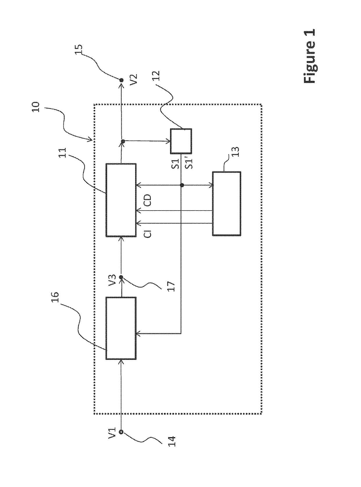
[0030]FIG. 1 shows a block diagram of an integrated calibration circuit according to a first aspect of the present invention. The calibration circuit which is denoted by reference symbol 10 is configured to calibrate the RC components of a filter circuit. The calibration circuit 10 comprises a chain of two filter circuits 11, 16, a saturation detector 12 and a calibration control logic 13.

[0031]In the embodiment of FIG. 1, the filter circuits 11, 16 are high-pass (HP) filters which are arranged in a signal path between an internal calibration input terminal 14 and an output terminal 15. A tap 17 having a tap voltage V3 is provided between the output side of the first HP filter 16 and the input side of the second HP filter 11.

[0032]A HP filter is an electronic device that let high frequency signals pass. HP-filter attenuate (which means reduces the amplitude of) signals with frequencies lower than the so-called cutoff frequency. The actual amount of attenuation for each frequency var...


PUM


Abstract

A calibration circuit and a method for calibrating a RC circuit, such as a high-pass filter, of an integrated circuit are provided. The calibration circuit comprises a filter arrangement having tuneable filter for filtering an input signal having a predetermined frequency. The filter comprises tuneable resistor elements, a saturation detector for detecting saturation and non-saturation of the tuneable filter by comparing a comparison voltage with the signal voltage of the filtered input signal, calibration control logic for providing incrementing and decrementing counter signals. The calibration circuit sets the comparison voltage to a first threshold voltage provides iteratively the incrementing counter signal to the filter until saturation is detected reduces the comparison voltage to a predetermined second threshold voltage after saturation is detected, the second threshold voltage being a lower value than the first threshold voltage, and provides the decrementing counter signal to the filter until non-saturation is detected.

Description

FIELD OF THE INVENTION[0001]This invention relates to a calibration circuit and a method for calibration of a filter circuit. The invention also relates to an integrated circuit, in particular a receiver circuit, and a radar system.BACKGROUND OF THE INVENTION[0002]Common technologies for producing integrated circuits are the so-called Complementary Metal Oxide Semiconductor (CMOS) and Bipolar Complementary Metal Oxide Semiconductor (BiCMOS). CMOS and / or BiCMOS technologies have become the fabrication technologies of choice for a majority of integrated circuits, such as automotive, cellular and wireless applications, due to its flexibility of design, level of integration and manufacturing costs. With (Bi)CMOS technology, however, there are also some limitations such as component tolerances. For example, component tolerances of on-chip passive integrated resistors and capacitors are typically in the range of + / −5% (best case), but more typically in the range of + / −30%. These component...

Claims


Application Information

Patent Timeline
Patent Type & Authority Patents(United States)
IPC IPC(8): H03H7/01H03H7/12G01S7/03
CPCH03H7/0161G01S7/032H03H7/12H03H2210/043H03H2210/036H03H2210/04H03H2210/028
Inventor PAVAO-MOREIRA, CRISTIANDOARE, OLIVIERGOUMBALLA, BIRAMA
Owner NXP USA INC
Why Eureka
Try Eureka