
Method and device for inspecting an optoelectronic component arranged on a connection board

a technology of optoelectronic components and connection boards, which is applied in the direction of measurement devices, electronic circuit testing, instruments, etc., can solve the problems of inability to operate with dc current, difficult to achieve the required field density using wire coils, and inability to selectively measure individual optoelectronic components, etc., to achieve better convergence of temporally variable alternating electromagnetic fields, improve the effect of field and simple production

Active Publication Date: 2019-05-14
OSRAM OLED
View PDF12 Cites 3 Cited by
  • Summary
  • Abstract
  • Description
  • Claims
  • Application Information

AI Technical Summary

Benefits of technology

This approach enables precise measurement of electro-optical properties, such as brightness and color, of individual optoelectronic components without exciting adjacent components, optimizing production processes and reducing rejects by allowing for better control over production steps like conversion material application.

Problems solved by technology

Consequently, these cannot be operated with DC current in order to determine their electro-optical properties for the purpose of process monitoring and / or process control.
A selective measurement, e.g., of the colour, of individual optoelectronic components is thus impossible.
In many cases, it is very difficult to achieve the required field density using wire coils which have a conventional geometry in terms of their winding.

Method used


Image

  • Method and device for inspecting an optoelectronic component arranged on a connection board
  • Method and device for inspecting an optoelectronic component arranged on a connection board
  • Method and device for inspecting an optoelectronic component arranged on a connection board

Examples


first embodiment

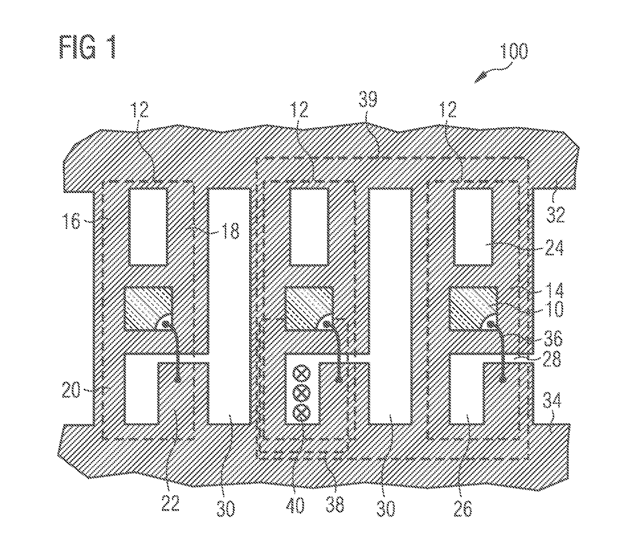
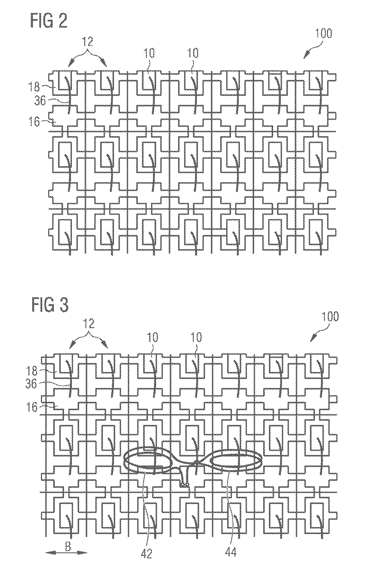
[0061]FIG. 3 schematically shows a method for inspecting an optoelectronic component. It shows the connection board 100 illustrated in FIG. 2, above or below which a double coil is arranged, which comprises a first coil 42 and a second coil 44. The arrangement of the double coil 42, 44 is illustrated only in diagrammatic form. The double coil 42, 44 generates a temporally variable electromagnetic alternating field, which induces an electrical alternating voltage in a local region of the connection board 100 and thus excites an electromagnetic resonant circuit. The excitation of the electromagnetic resonant circuit here takes place in a manner similar to that already explained in association with FIG. 1. The first coil 42 and the second coil 44 are spaced apart from one another laterally, more specifically in a direction parallel to a main extension plane of the connection board 100 and perpendicular to the central axes or axes of symmetry of the two coils 42, 44. A distance between ...

second embodiment

[0064]FIG. 4 schematically shows a method for inspecting an optoelectronic component. In this embodiment, in addition to the coils 42, 44, electrical contacts 46, e.g., needle contacts or pogo pins, are provided, which are arranged such that short circuit paths are generated on the connection board 100. As a result, defined current paths are obtained and, e.g., undesired leakage current paths are reduced.

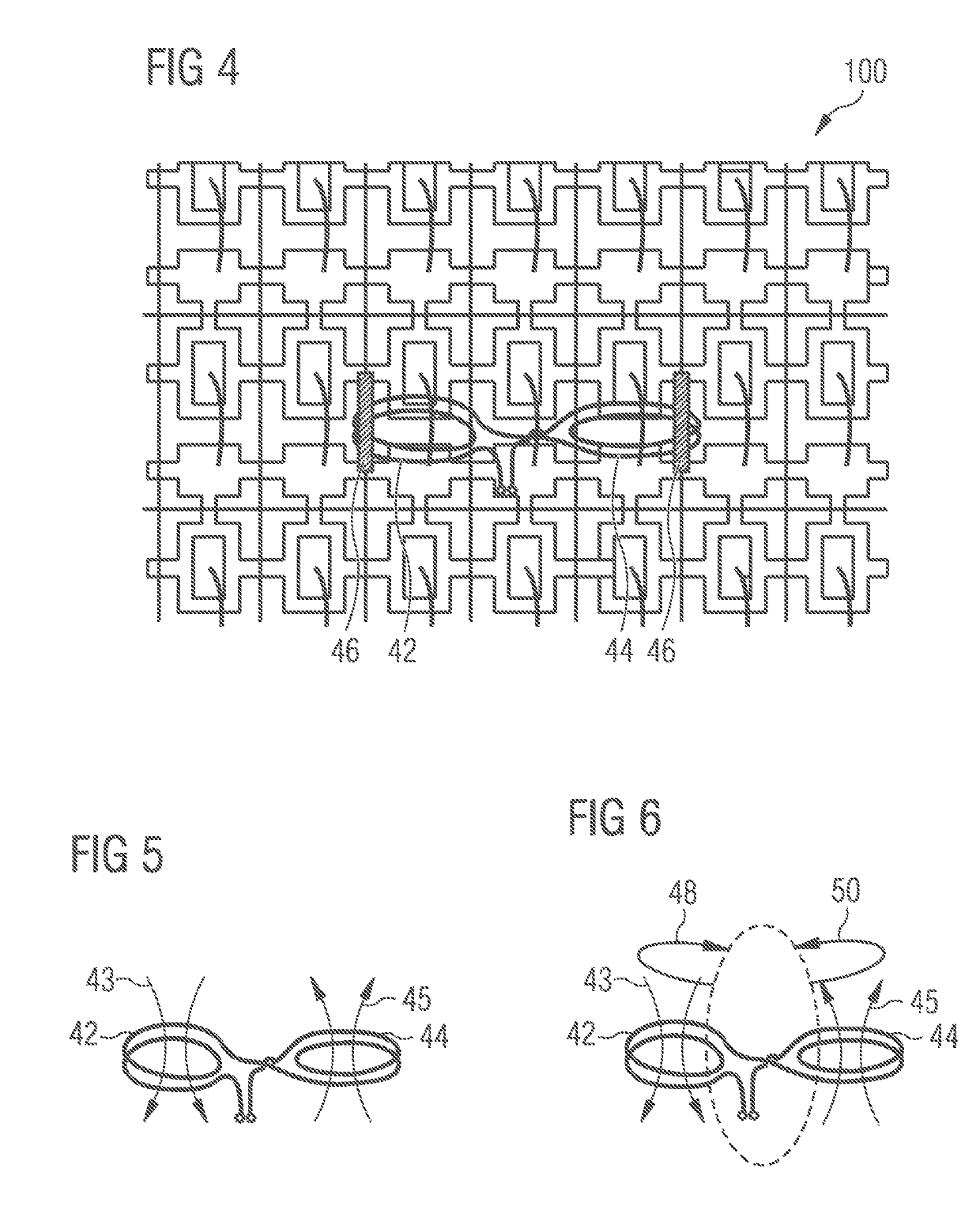
[0065]FIGS. 5 and 6 schematically show the portions of the magnetic field 43, 45 generated by the two coils 42, 44. The two coils 42, 44 are wound in opposite directions, such that the magnetic field 43 inside the first coil 42 is always directed antiparallel to the magnetic field 45 inside the second coil 44. As a result, two voltages 48, 50 having opposite rotational directions are induced by the two coils on the connection board, which voltages add in a region in the center between the two coils 42, 44. An electromagnetic resonant circuit is or electromagnetic resonant circuits a...

third embodiment

[0066]FIG. 7 shows a diagram of a flat coil 52 for use in a method for inspecting an optoelectronic component. The flat coil 52 is formed by a wound metal wire, has the shape of an Archimedean spiral and in the present case has four windings. An even better field convergence can be obtained by means of a higher number of windings. Alternatively or additionally, an increase in the generated field strength can also be achieved by the arrangement of a ferrite core 54 in the center of the flat coil 52 (see FIG. 8).

[0067]FIGS. 9 to 11 show embodiments in which the flat coil 52 is formed by a patterned circuit board. An arrangement of this type can be produced in particular by photochemical etching of a circuit board. Depending on the part size and available space, the use of a ferromagnetic element for additional field convergence is also feasible.

[0068]FIGS. 10 and 11 show special embodiments in which selective excitation of one or a few optoelectronic components on the connection board...


PUM


Abstract

A method and a device for inspecting an optoelectronic component are disclosed. In an embodiment, the method includes exciting at least one electromagnetic resonant circuit, formed by the at least one optoelectronic component and the connection board, such that the at least one optoelectronic component emits electromagnetic radiation, wherein exciting the electromagnetic resonant circuit comprises applying an electrical alternating voltage in the electromagnetic resonant circuit by generating a temporally variable electromagnetic alternating field by a first coil and a second coil, wherein the first coil and the second coil are movable with respect to the connection board.

Description

[0001]This patent application is a national phase filing under section 371 of PCT / EP2016 / 050691, filed Jan. 14, 2016, which claims the priority of German patent application 10 2015 101 671.0, filed Feb. 5, 2015, each of which is incorporated herein by reference in its entirety.TECHNICAL FIELD[0002]A method and a device for inspecting an optoelectronic component arranged on a connection board are provided.BACKGROUND[0003]The measurement of electro-optical properties of optoelectronic components generally takes place according to the prior art by applying a DC voltage to the optoelectronic component. Occasionally, optoelectronic components are at least temporarily present in a form in which their connections are short-circuited, that is to say in which there is a negligible ohmic resistance between their connections. This is the case particularly if optoelectronic components are arranged on a connection board, e.g., during the production of optoelectronic components. For example, opto...

Claims


Application Information

Patent Timeline
Patent Type & Authority Patents(United States)
IPC IPC(8): G01R31/26G01R31/28
CPCG01R31/2831G01R31/2635
Inventor SCHULZ, ROBERTVOGL, ANTONZEISEL, ROLAND
Owner OSRAM OLED
Learn More