Isolation structure for micro-transfer-printable devices

a technology of integrated circuits and isolating structures, which is applied in the direction of solid-state devices, basic electric elements, electric devices, etc., can solve problems such as difficulty in achieving, and achieve the effects of efficient forming of robust releasable integrated circuits, high resolution, and easy production

Active Publication Date: 2019-05-21
X FAB SEMICON FOUNDRIES +1
View PDF152 Cites 2 Cited by
  • Summary
  • Abstract
  • Description
  • Claims
  • Application Information

AI Technical Summary

Benefits of technology

[0015]The present invention provides structures and methods for efficiently forming robust releasable integrated circuits for micro-transfer printing in a cost-effective manner. Furthermore, when compared to other manufacturing methods, the present invention enables higher resolution tethers that are more easily made because the tether structures are constructed early in the process before the semiconductor devices are formed. The semiconductor devices are also more robust and less prone to process difficulties because the number of process steps performed to make a micro-transfer printable device after the device is constructed is consequently reduced. Furthermore, semiconductor devices made according to methods of the present invention can be arranged at a higher density on a wafer since multiple etching operations are unnecessary after the semiconductor devices are constructed, providing a more efficient and cost-effective use of expensive wafers.

Problems solved by technology

However, this can be difficult to accomplish when the integrated circuits are small.

Method used


Image

  • Isolation structure for micro-transfer-printable devices
  • Isolation structure for micro-transfer-printable devices
  • Isolation structure for micro-transfer-printable devices

Examples


Embodiment Construction

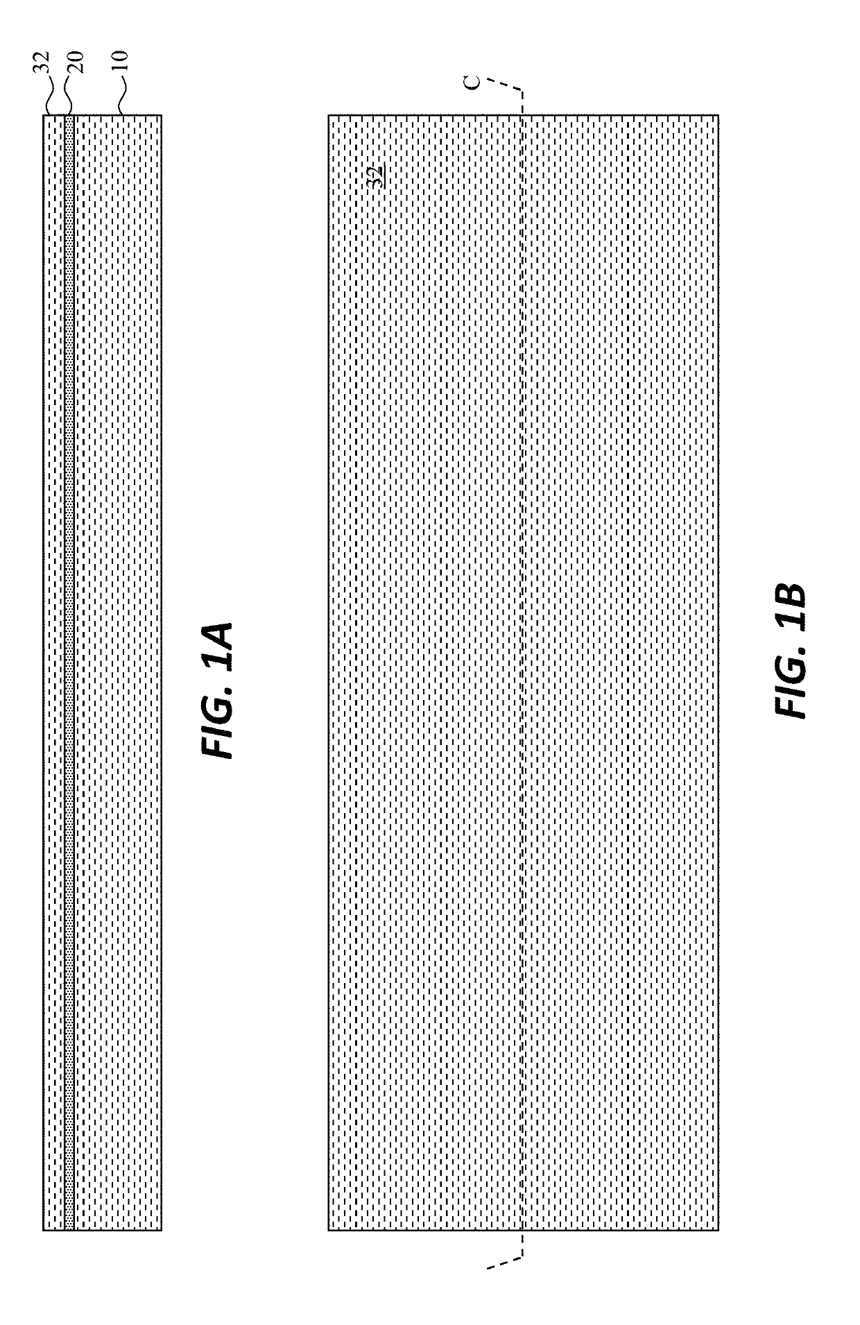
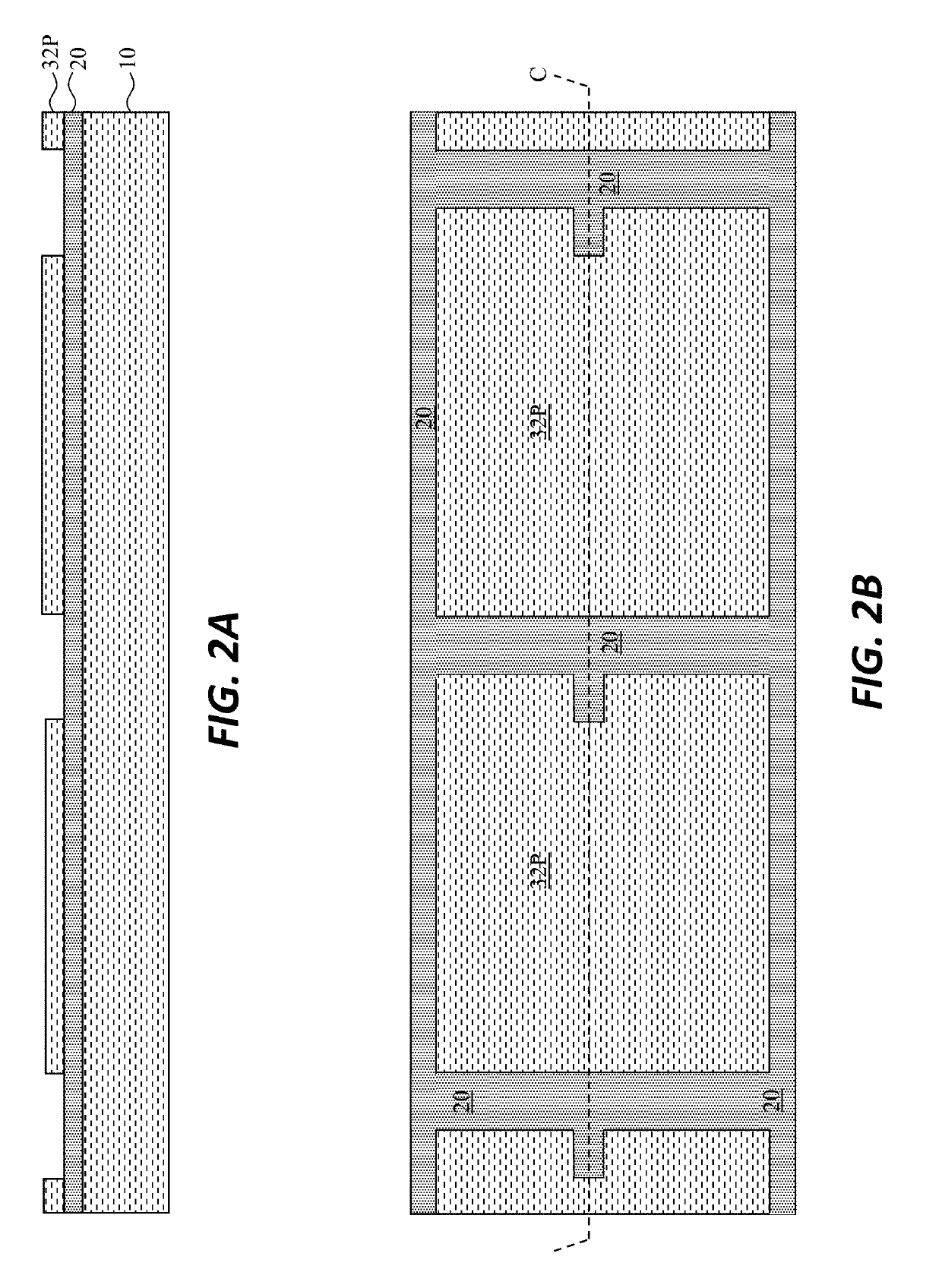
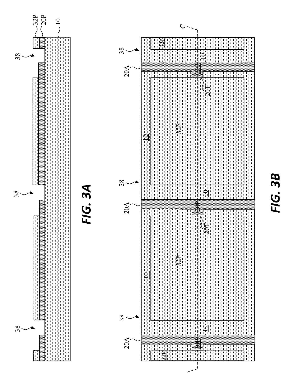
[0067]Embodiments of the present invention provide structures and methods for efficiently forming robust releasable integrated circuits for micro-transfer printing in a cost-effective manner. The integrated circuits are surrounded by an isolation layer that provides environmental and electrical protection to the device. Methods of the present invention provide reduced processing steps to make such robust releasable or released integrated circuits suitable for micro-transfer printing using a stamp. Moreover, embodiments of the present invention provide structures and methods to enable micro-transfer printing from devices formed on alternative substrates or disposed on handle substrates that include materials different from materials in the integrated circuits.

[0068]FIGS. 1-11 illustrate successive sequential steps and structures for making embodiments of the present invention. Each Figure includes a plan view from the top (B) and a corresponding cross section (A) taken across the cro...


PUM


Abstract

A semiconductor structure suitable for micro-transfer printing includes a semiconductor substrate and a patterned insulation layer disposed on or over the semiconductor substrate. The insulation layer pattern forms one or more etch vias in contact with the semiconductor substrate. Each etch via is exposed. A semiconductor device is disposed on the patterned insulation layer and is surrounded by an isolation material in one or more isolation vias that are adjacent to the etch via. The etch via can be at least partially filled with a semiconductor material that is etchable with a common etchant as the semiconductor substrate. Alternatively, the etch via is empty and the semiconductor substrate is patterned to form a gap that separates at least a part of the semiconductor device from the semiconductor substrate and forms a tether physically connecting the semiconductor device to an anchor portion of the semiconductor substrate or the patterned insulation layer.

Description

PRIORITY APPLICATION[0001]This application claims priority to and benefit of U.S. Patent Application No. 62 / 436,038, filed Dec. 19, 2016, entitled Isolation Structure for Micro-Transfer Printable Devices, the content of which is hereby incorporated by reference in its entirety.FIELD OF THE INVENTION[0002]The present invention relates to structures and methods for providing micro-transfer printable integrated circuits on semiconductor substrates using isolation structures.BACKGROUND OF THE INVENTION[0003]Integrated circuits (ICs) are widely used in electronic devices. Integrated circuits are typically formed on a semiconductor wafer using photolithographic processes and then packaged, for example in a ceramic or plastic package, with pins or bumps on the package providing externally accessible electrical connections to the integrated circuit.[0004]In some applications, the bare integrated circuit dies are not separately packaged but are placed on a destination substrate and electrica...

Claims


Application Information

Patent Timeline
Patent Type & Authority Patents(United States)
IPC IPC(8): H01L25/00H01L21/78H01L21/762H01L21/683H01L21/84
CPCH01L21/7806H01L21/6835H01L21/76283H01L21/84H01L25/50H01L2221/68381H01L2221/6835H01L2221/68318H01L2221/68354H01L2221/68368
Inventor BOWER, CHRISTOPHER ANDREWCOK, RONALD S.NEVIN, WILLIAM ANDREWKITTLER, GABRIEL
Owner X FAB SEMICON FOUNDRIES
Why Eureka
Try Eureka