Semiconductor device and manufacturing method therefor

a technology of semiconductors and manufacturing methods, applied in the field of semiconductor devices, can solve the problems of affecting the reliability of such electronic components, the gidl of gated-induced drains is relatively large, and the short channel effect (sce) becomes more serious, and achieves the effect of reducing the gidl of an electronic componen

Active Publication Date: 2019-09-17
SEMICON MFG INT (SHANGHAI) CORP +1
View PDF2 Cites 0 Cited by
  • Summary
  • Abstract
  • Description
  • Claims
  • Application Information

AI Technical Summary

Benefits of technology

[0024]In the semiconductor device provided in this application, the thickness of a first region at which a first gate dielectric layer abuts against a first drain region is greater than that of an intermediate third region. That is, the thickness of the first gate dielectric layer between overlapping portions of the first drain region and the first gate in increased, so as to reduce a vertical electric-field strength, and decrease GIDL of an electronic component.

Problems solved by technology

As critical dimensions of a metal oxide semiconductor field effect transistor (MOSFET) decrease, the short channel effect (SCE) becomes more serious.
However, for some FinFET electronic components, such as an input / output (I / O) electronic component, a gated-induce drain leakage (GIDL) is relatively large.
Therefore, reliability of such electronic components may be affected.

Method used


Image

  • Semiconductor device and manufacturing method therefor
  • Semiconductor device and manufacturing method therefor
  • Semiconductor device and manufacturing method therefor

Examples


Embodiment Construction

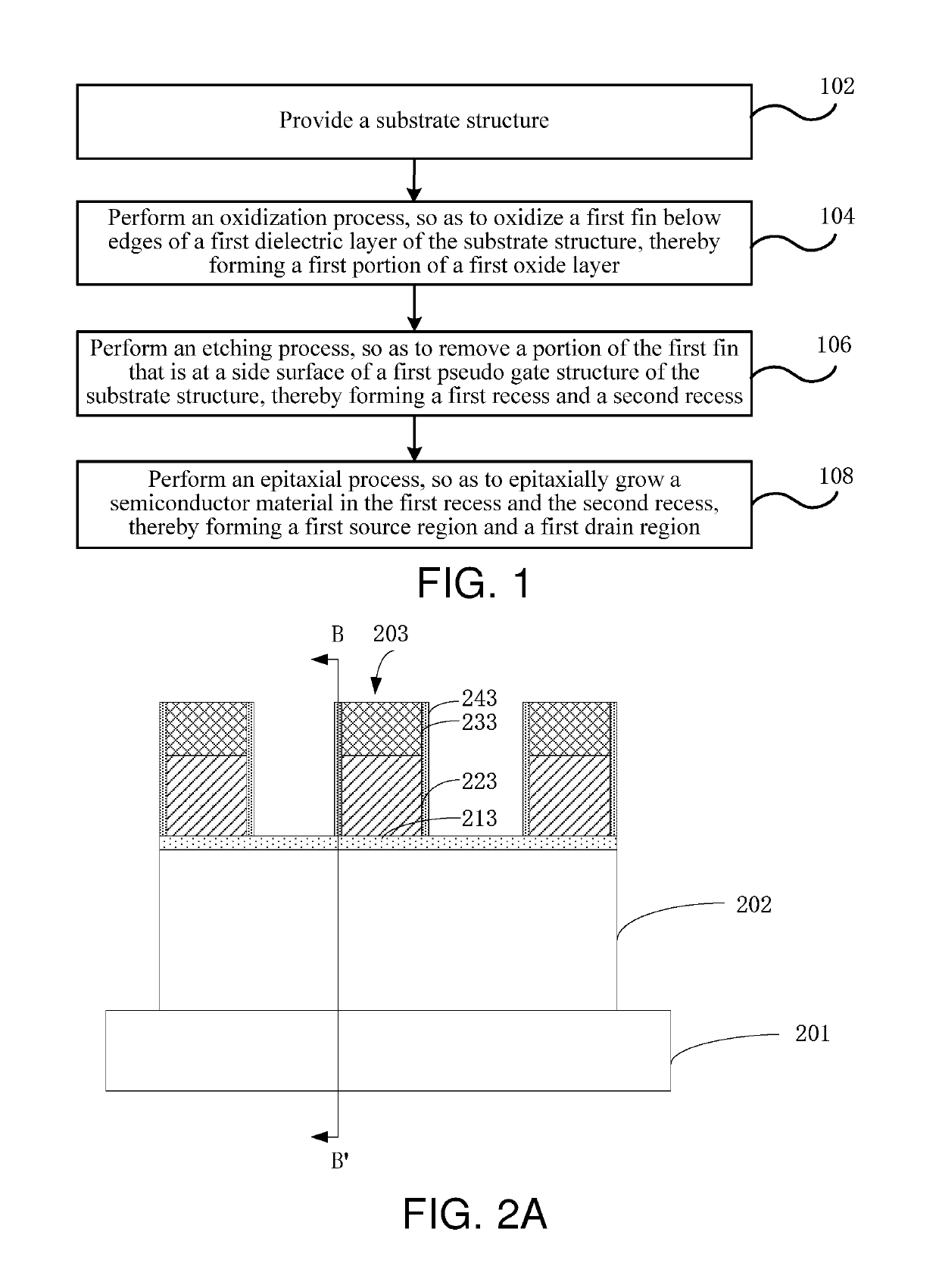
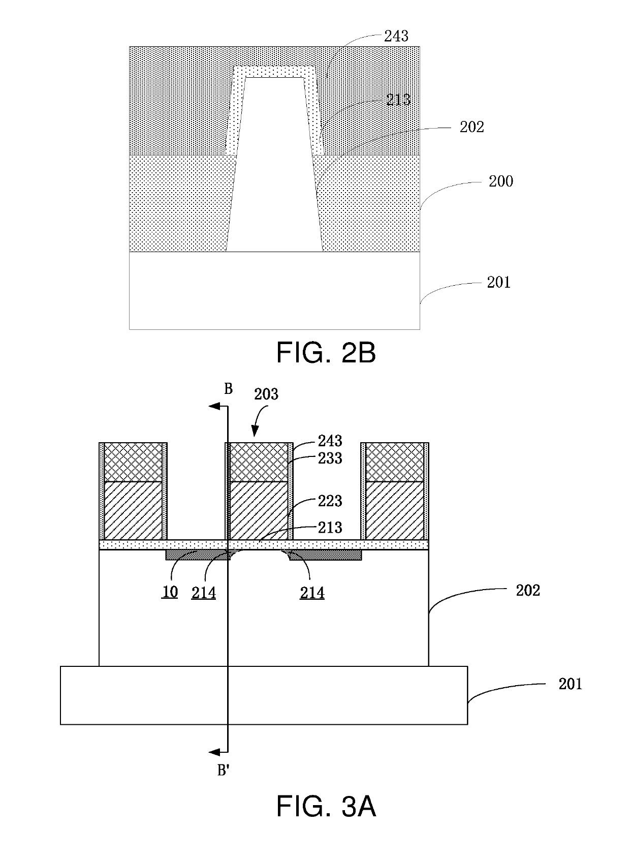
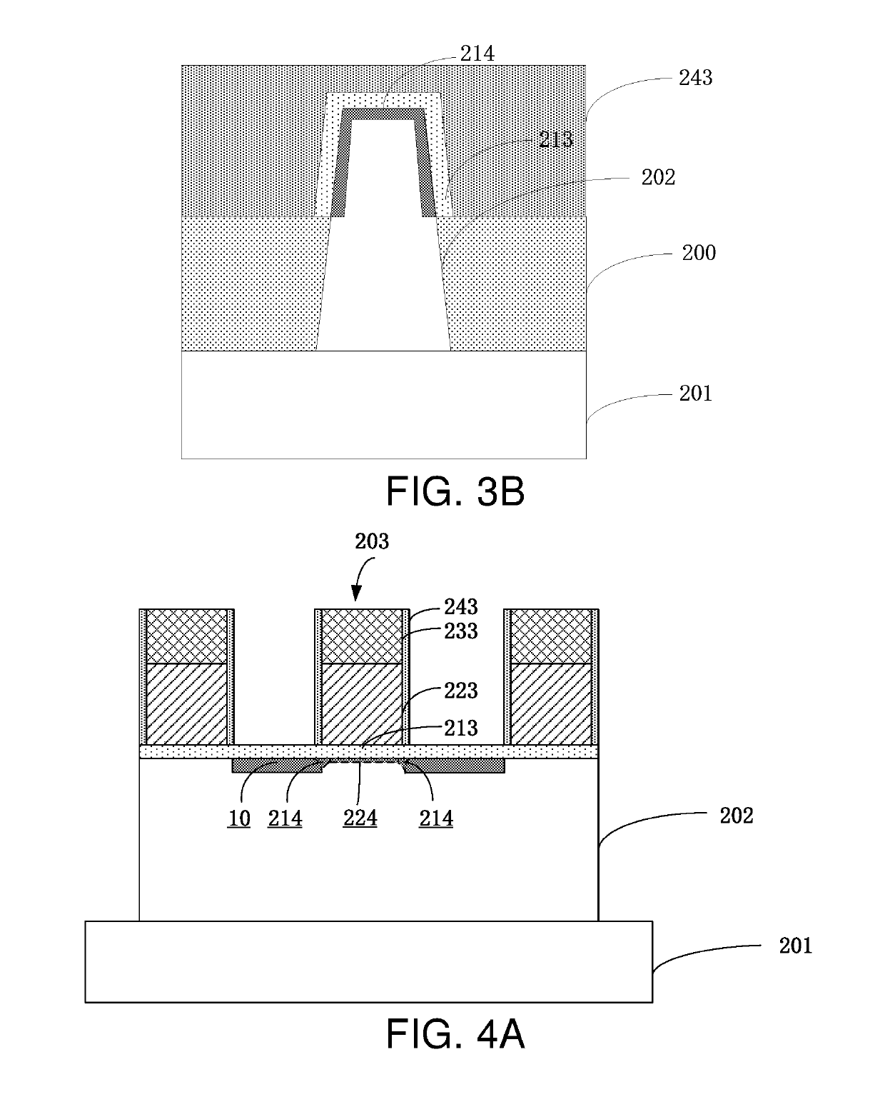
[0031]Exemplary implementations are described in detail with reference to the accompanying drawings. It should be understood that unless otherwise specified, relative layouts, mathematical expressions, and numeric values of components and steps described in these implementations should not be understood as a limitation to the scope of this disclosure.

[0032]In addition, it should be understood that for ease of description, sizes of the components shown in the accompanying drawings are not necessarily drawn according to an actual proportional relationship. For example, thicknesses or widths of some layers may be magnified with respect to other layers.

[0033]The following descriptions of the exemplary implementations are only illustrative, and would not be used as any limitation on the scope of this disclosure and on the applications or uses of this disclosure in any sense.

[0034]Technologies, methods, and devices that are known by a person of ordinary skill in the related fields may not...


PUM


Abstract

This disclosure relates to the technical field of semiconductors, and discloses a semiconductor device and a manufacturing method therefor. The semiconductor device may include a substrate; a first fin on the substrate for forming a first electronic component; a first gate structure on a portion of the first fin including a first gate dielectric layer on a portion of the first fin and a first gate on the first gate dielectric layer; and a first source region and a first drain region that each at one of two sides of the first gate structure and at least partially located in the first fin, where the first gate dielectric layer comprises a first region abutting against the first drain region, a second region abutting against the first source region, and a third region between the first region and the second region, and wherein thickness of the first region is greater than that of the third region.

Description

RELATED APPLICATIONS[0001]The present application claims priority to Chinese Patent Application No. 201710350094.9, filed on May 18, 2017, the entire disclosure of which is hereby incorporated by reference.BACKGROUNDTechnical Field[0002]This disclosure relates to the technical field of semiconductors, and in particular, to a semiconductor device and a manufacturing method therefor.Related Art[0003]As critical dimensions of a metal oxide semiconductor field effect transistor (MOSFET) decrease, the short channel effect (SCE) becomes more serious. A fin field effect transistor (FinFET) has improved gate control capabilities, and can effectively reduce the SCE.[0004]However, for some FinFET electronic components, such as an input / output (I / O) electronic component, a gated-induce drain leakage (GIDL) is relatively large. Therefore, reliability of such electronic components may be affected.SUMMARY[0005]An objective of this disclosure is to decrease GIDL of an electronic component.[0006]In...

Claims


Application Information

Patent Timeline
Patent Type & Authority Patents(United States)
IPC IPC(8): H01L29/04H01L21/28H01L29/08H01L27/088H01L29/423H01L21/8234
CPCH01L29/42368H01L29/0847H01L21/823462H01L21/28211H01L27/0886H01L21/823418H01L21/823431H01L29/66545H01L29/66795H01L29/785H01L29/7853
Inventor LI, YONGHONG, ZHONGSHAN
Owner SEMICON MFG INT (SHANGHAI) CORP
Why Eureka
Try Eureka