Method of forming word wire of semiconductor

A semiconductor and device technology, applied in the field of word lines forming semiconductor devices, can solve problems such as charge loss and lower refresh characteristics of devices

Inactive Publication Date: 2004-02-18
SK HYNIX INC
View PDF0 Cites 0 Cited by
  • Summary
  • Abstract
  • Description
  • Claims
  • Application Information

AI Technical Summary

Problems solved by technology

Overlap produces gate-induced drain leakage ("GIDL") due to the voltage difference between the word line and the source / drain region, which causes the charge stored in the capacitor to be lost, degrading the device The refresh feature of

Method used


Image

  • Method of forming word wire of semiconductor
  • Method of forming word wire of semiconductor
  • Method of forming word wire of semiconductor

Examples


Embodiment Construction

[0019] The present invention will be described in detail with reference to the drawings.

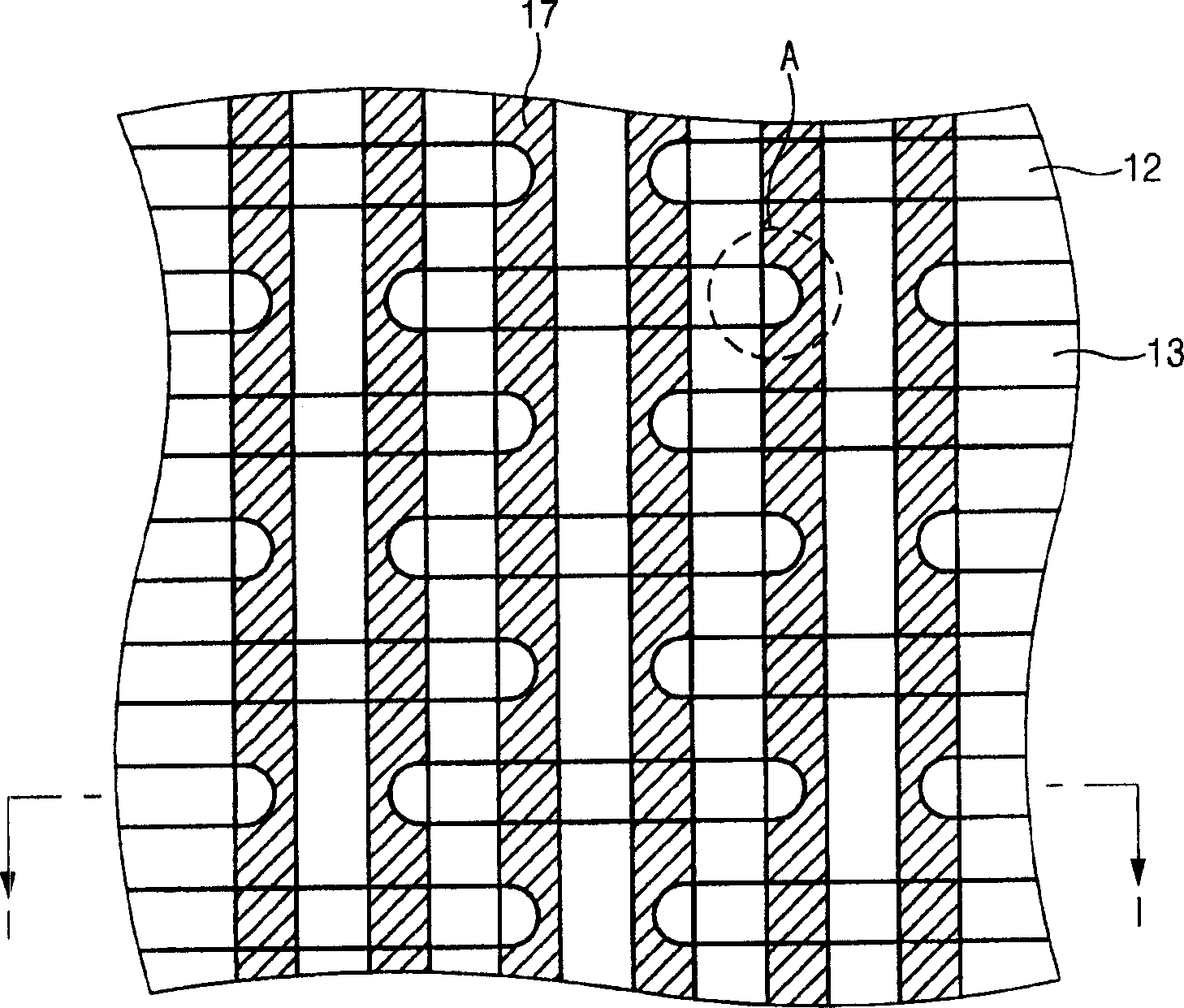
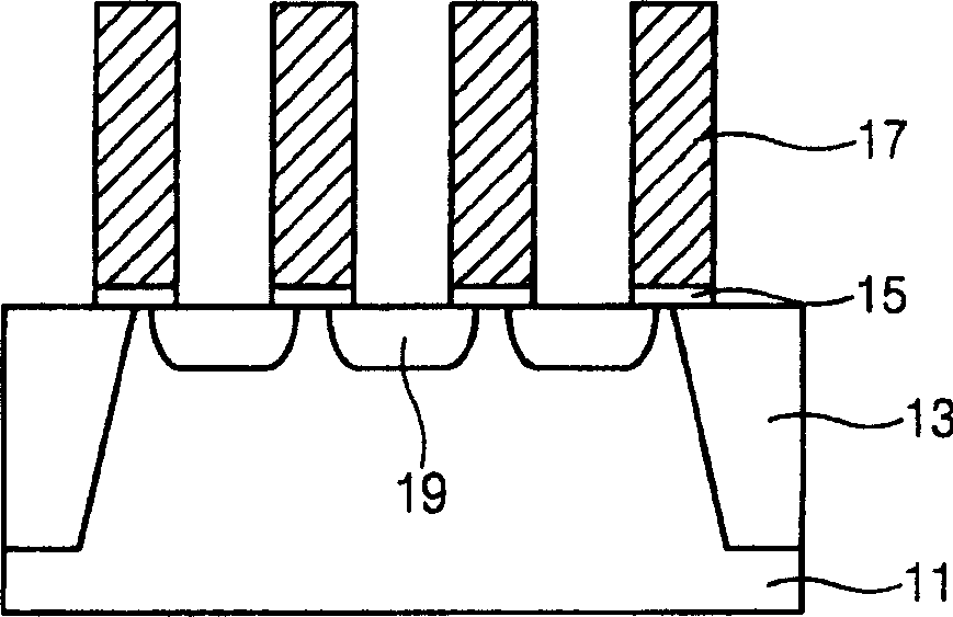
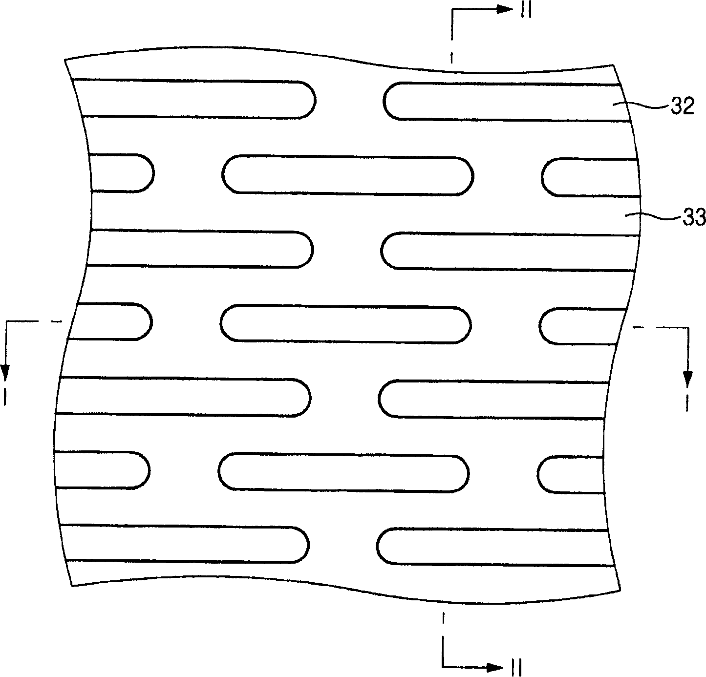
[0020] Figures 3a to 3d is a layout diagram showing a method of forming word lines according to an embodiment of the present invention. Figures 4a to 4d are along Figures 3a to 3d Sectional view of lines I-I and II-II.

[0021] refer to Figure 3a and 4a The device isolation film 33 defining the I-type active region 32 is formed by performing a shallow trench isolation process in the device isolation region of the p-type semiconductor substrate 31 . The active regions 32 are separated from each other by a predetermined distance in the horizontal direction, and are staggered in the vertical direction.

[0022] refer to Figure 3b and 4b , a sacrificial insulating film (not shown), preferably a nitride film, is formed on the semiconductor substrate 31 . The sacrificial insulating film is selectively etched to form an I-type sacrificial insulating film pattern 35 on a predetermin...


PUM


Abstract

A method for forming word line of semiconductor device wherein a lower portion of the word line on the channel region is a I-type and a upper portion of the word line is a line-type is disclosed. The method comprises (a) forming a sacrificial insulation film on a semiconductor substrate including an active region; (b) etching the sacrificial insulation film to form an I-type sacrificial insulation film pattern whereon a channel region is to be formed; (c) forming a source / drain region; (d) forming a first interlayer insulation film; (e) planarizing the first interlayer insulation film to expose the sacrificial insulation film pattern; (f) sequentially forming a insulation film and a second interlayer insulation film; (g) etching the second interlayer insulation film and insulation film using a word line mask; (h) removing the sacrificial insulation film pattern; (i) growing a gate oxide film; (j) forming a conductive layer; and (k) planarizing the conductive layer.

Description

technical field [0001] The present invention generally relates to a method of forming a word line of a semiconductor device, and more particularly, to a method of forming a word line of a semiconductor device, wherein the lower part of the word line on the channel region is I-type, and the upper part of the word line It is a linear type, which is beneficial to improve the characteristics, yield and reliability of the device. Background technique [0002] figure 1 is the layout diagram of conventional word lines, figure 2 is along figure 1 Sectional view of the I-I line. [0003] refer to figure 1 and 2 , the gate electrode 17 has a gate oxide film 15, which is disposed on the p-type semiconductor substrate 11, the substrate 11 has a device isolation film 13, the isolation film 13 defines the active region 12, and the source / drain region 19 is disposed on Both sides of the gate electrode 17 on the semiconductor substrate 11 . [0004] The active regions 12 are arrange...

Claims


Application Information

Patent Timeline
Patent Type & Authority Applications(China)
IPC IPC(8): H01L21/28H01L21/336H01L21/768
CPCH01L29/66545H01L21/76801H01L21/28
Inventor 李元畅
Owner SK HYNIX INC
Why Eureka
Try Eureka