
Standard cell architecture with at least one gate contact over an active area

a gate contact and active area technology, applied in the field of semiconductor devices, can solve the problems of wide performance differences between devices, limited performance of standard semiconductor cell libraries, and approach producing additional disadvantages, so as to reduce the number of metal layers, improve the access of pins, and shorten the cell height

Active Publication Date: 2019-09-24
INT BUSINESS MASCH CORP
View PDF19 Cites 0 Cited by
  • Summary
  • Abstract
  • Description
  • Claims
  • Application Information

AI Technical Summary

Benefits of technology

The patent text describes a method for improving semiconductor device performance by using a reduced number of metal layers and optimizing the placement of gate contacts. This leads to better pin access, reduced cell height, and improved device width. Additionally, the use of a new material called AUXFIN helps to minimize process and yield risks, while eliminating the need for a specific metal layer and simplifying cell connectivity schemes. Ultimately, this method reduces manufacturing costs.

Problems solved by technology

Standard semiconductor cell library performance is limited by the current a transistor of a cell can deliver.
The devices also exhibit wide performance differences due to semiconductor process variations.
However, this approach produces additional disadvantages.
This known prior art approach increases the parasitic coupling significantly, thereby slowing down circuit performance.
The amount of silicon needed to implement the cells increases as the design rules are restricted.
This additional metal 2 (M2 layer) routing within the cells also adversely uses most of the available metal 2 (M2 layer) connectivity resources.
Further, because the base cells now include the M2 layer, a routing congestion issue can occur when trying to route inter-cell connection signals, or power, clock or ground signals, over the cells.
These solutions to congestion in the cells add to manufacturing costs.

Method used


Image

  • Standard cell architecture with at least one gate contact over an active area
  • Standard cell architecture with at least one gate contact over an active area
  • Standard cell architecture with at least one gate contact over an active area

Examples


Embodiment Construction

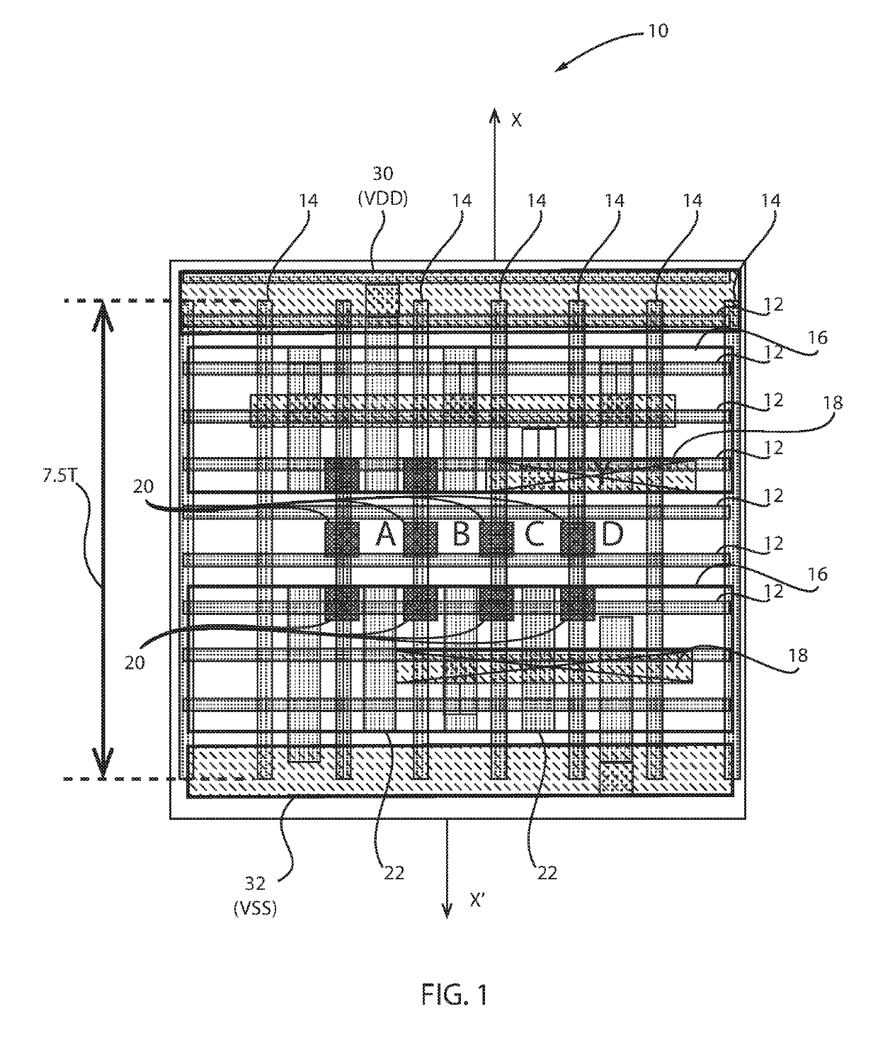
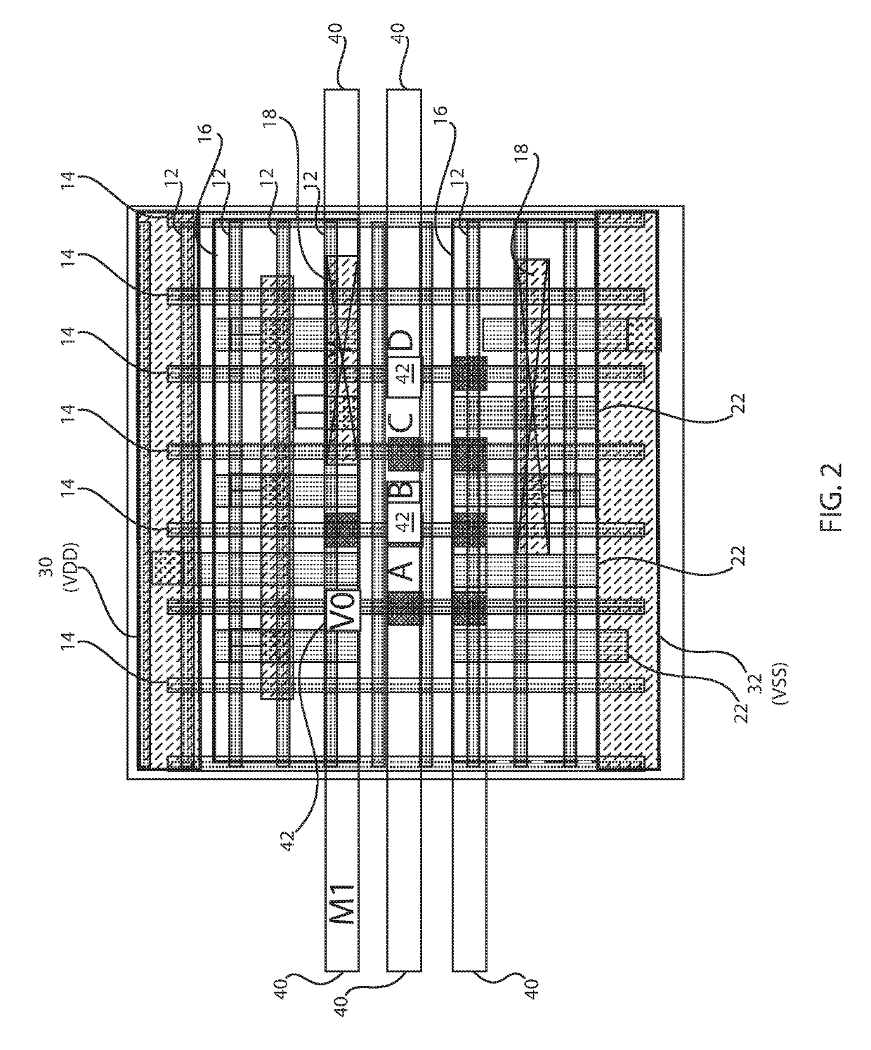
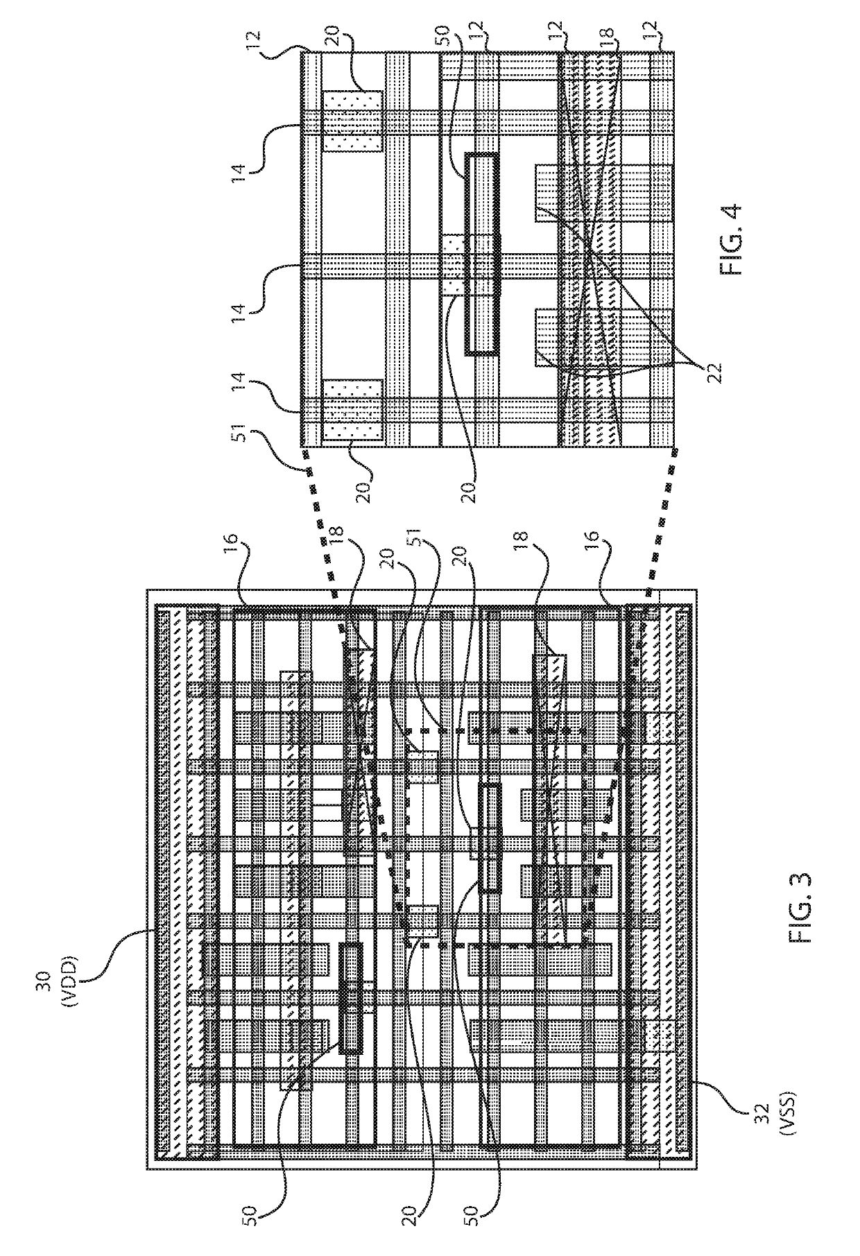
[0031]In accordance with an embodiment, a method is provided for forming a layout of a standard cell. The method includes forming a plurality of gate conductors, forming a plurality of active areas, and forming at least one gate contact (CB contact) within an active region of the plurality of active regions.

[0032]In accordance with another embodiment, a layout of a standard cell is provided. The layout of the standard cell includes a plurality of gate conductors, a plurality of active areas, and at least one gate contact (CB contact) formed within an active region of the plurality of active regions.

[0033]In one or more embodiments, a new and useful logic standard cell architecture is presented that advantageously leverages gate contacts over active regions to reduce the number of metals used while improving pin access. In addition, effective device width (i.e., number of fins) can be maximized to improve performance. AUXFIN is also introduced as a complete and useful design solution...


PUM


Abstract

A method is presented for forming a layout of a MOSFET (metal oxide semiconductor field effect transistor) circuit. The method includes forming a plurality of gate conductors, forming a plurality of active areas, and forming at least one gate contact (CB contact) within an active region of the plurality of active regions. The method further includes placing a marker over the at least one gate contact to identify a location of the at least one gate contact. Additionally, a distance between the at least one gate contact and at least one TS contact is optimized based on device specifications.

Description

BACKGROUNDTechnical Field[0001]The present invention relates generally to semiconductor devices, and more specifically, to structures and methods of fabricating semiconductor devices using standard semiconductor cell fabrication.Description of the Related Art[0002]Standard semiconductor cell fabrication is a method for designing integrated circuits (ICs) for specific applications. Circuits are designed based on the desired functions using cells from a cell library, which are combined and constructed by a placement tool to result in the desired circuits. Standard semiconductor cell library performance is limited by the current a transistor of a cell can deliver. This is proportional to the width of the transistor. Thus, it is desirable to enable the transistor to be as wide as possible in a standard cell to deliver high performance circuits.[0003]Standard cell methodology is a technique of designing ICs with a focus on the logic functions used in the IC. A standard cell includes mult...

Claims


Application Information

Patent Timeline
Patent Type & Authority Patents(United States)
IPC IPC(8): G06F17/50H01L27/02H01L27/118
CPCH01L27/11807G06F17/5072G06F17/5077H01L27/0207H01L2027/11866G06F30/39G06F30/392G06F30/394
Inventor CHU, ALBERT M.NA, MYUNG-HEERAMACHANDRAN, RAVIKUMAR
Owner INT BUSINESS MASCH CORP
Learn More