Voltage abnormality detection circuit and semiconductor device
a voltage abnormality and circuit technology, applied in the direction of power supply testing, measurement devices, instruments, etc., can solve the problem of not being able to detect abnormalities in the circuit of voltage regulators, and achieve the effect of simple circuit configuration
- Summary
- Abstract
- Description
- Claims
- Application Information
AI Technical Summary
Benefits of technology
Problems solved by technology
Method used
Image


Examples
first embodiment
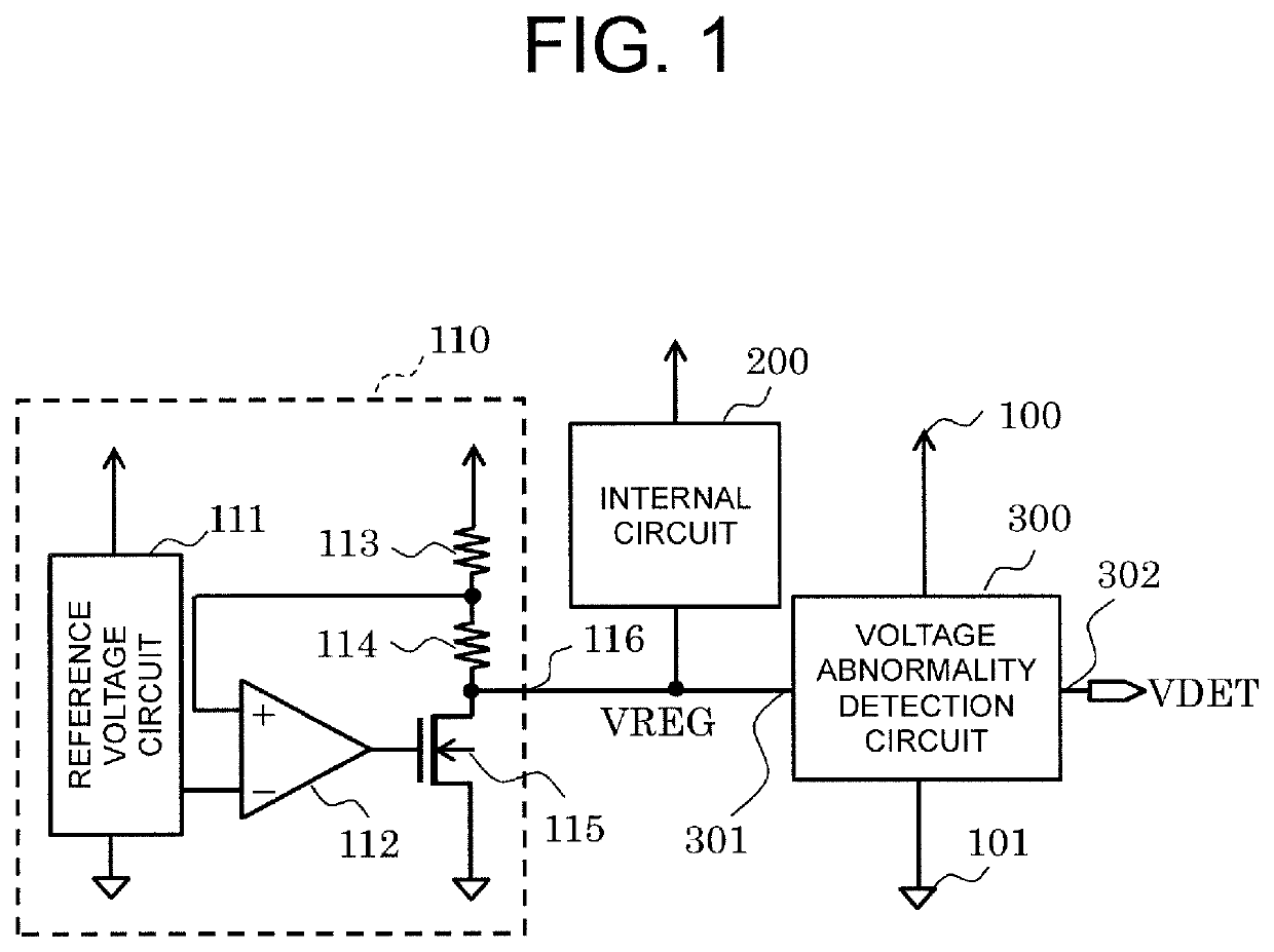
[0024]FIG. 2 is a circuit diagram for illustrating a voltage abnormality detection circuit according to a first embodiment of the present invention.
[0025]A voltage abnormality detection circuit 300a according to the first embodiment includes a reference voltage circuit 310, a first voltage detection circuit 321, a second voltage detection circuit 322, an inverter circuit 371, and an OR circuit 372. The reference voltage circuit 310 is configured to output a first reference voltage which is higher than a desired internal power supply voltage, and a second reference voltage which is lower than the desired internal power supply voltage.
[0026]The first voltage detection circuit 321 includes a first input terminal to which the first reference voltage of the reference voltage circuit 310 is input, and a second input terminal to which the voltage of the input terminal 301, namely, the constant voltage VREG, is input. The second voltage detection circuit 322 includes a first input terminal ...
second embodiment
[0038]FIG. 4 is a circuit diagram for illustrating a voltage abnormality detection circuit according to a second embodiment of the present invention. The difference from the voltage abnormality detection circuit 300a according to the first embodiment is that a switch circuit, which includes switches 401, 402, 403, and 404, is added.
[0039]One end of the switch 401 is connected to a first output terminal of the reference voltage circuit 310, and the other end of the switch 401 is connected to the first input terminal of the first voltage detection circuit 321. One end of the switch 402 is connected to the first output terminal of the reference voltage circuit 310, and the other end of the switch 402 is connected to the first input terminal of the second voltage detection circuit 322. One end of the switch 403 is connected to a second output terminal of the reference voltage circuit 310, and the other end of the switch 403 is connected to the first input terminal of the first voltage d...
PUM
| Property | Measurement | Unit |
|---|---|---|
| voltage | aaaaa | aaaaa |
| current | aaaaa | aaaaa |
| constant current | aaaaa | aaaaa |
Abstract
Description
Claims
Application Information