Supercharge Your Innovation With Domain-Expert AI Agents!

Semiconductor logic device and system and method of embedded packaging of same

a logic device and semiconductor technology, applied in semiconductor devices, semiconductor/solid-state device details, electrical apparatus, etc., can solve the problems of low electrical conductivity, low resistance loss of solder bumps, and fewer chips per chip

Active Publication Date: 2020-02-18
GENERAL ELECTRIC CO
View PDF73 Cites 0 Cited by
  • Summary
  • Abstract
  • Description
  • Claims
  • Application Information

AI Technical Summary

Benefits of technology

Enables a 20-30% die size reduction and 15-20% cost reduction while maintaining or improving power delivery and reliability, with a ten-fold reduction in interconnect resistance and a four-fold increase in current carrying capability compared to traditional flip chip solder bump approaches.

Problems solved by technology

Typically, high-end semiconductor logic chips have 70 to 85 percent of all I / O pads dedicated to power and ground due to high power / ground current levels in these devices and performance limitations of the solder bumps.
Solder bumps have high resistance losses due to their low electrically conductivity and current limitations due to electro-migration susceptibility.
Larger chips result in fewer chips per wafer and lower wafer level chip yields, which increases the cost of the chip.
Despite the ever-evolving push for device miniaturization, many flip chip devices with high I / O pad counts cannot reduce the die size when moving to a smaller feature node because of the minimum pitch allowable on solder bumped flip chip devices.
Reducing the array grid pitch is particularly problematic in flip chip solder ball attach.
A tighter grid pitch would require smaller I / O pads, smaller solder bumps, and would have lower bump conductivity, higher assembly costs, higher risk of bump-to-bump shorting, and lower solder fatigue compliance.
As a result, designers may move a flip chip device that is pad count limited to a smaller semiconductor node to get improved device performance but the die size could not be shrunk without lower assembly yield, lower device reliability and increased costs.
While copper pillars can be used on a tighter pitch than the minimum solderable pitch without causing a pad-to-pad short, shrinking the pitch of a copper pillar / solder layer flip chip attach structure increases the risk of electro-migration failures.
One key problem with utilizing embedded chip packaging is that the interconnect structure built over the chip has a yield loss due to interconnect fabrication defects such as shorts and opens.
A defect in the interconnect structure that is formed after a chip is embedded in the structure would cause the chip to be scrapped along with the defective interconnect structure.
Complex semiconductor logic devices with high numbers of I / O pads, on the other hand, require complex interconnect structures with unacceptable yield losses of 20% or higher.
A 20% embedded chip yield loss would cause 20% of the complex chips to be scrapped with the defective interconnect structures in which they are embedded.
For these reasons, the implementation of embedded chip technologies to complex semiconductor logic devices has been restricted and has not been done in high volume manufacturing.

Method used


Image

  • Semiconductor logic device and system and method of embedded packaging of same
  • Semiconductor logic device and system and method of embedded packaging of same
  • Semiconductor logic device and system and method of embedded packaging of same

Examples


Embodiment Construction

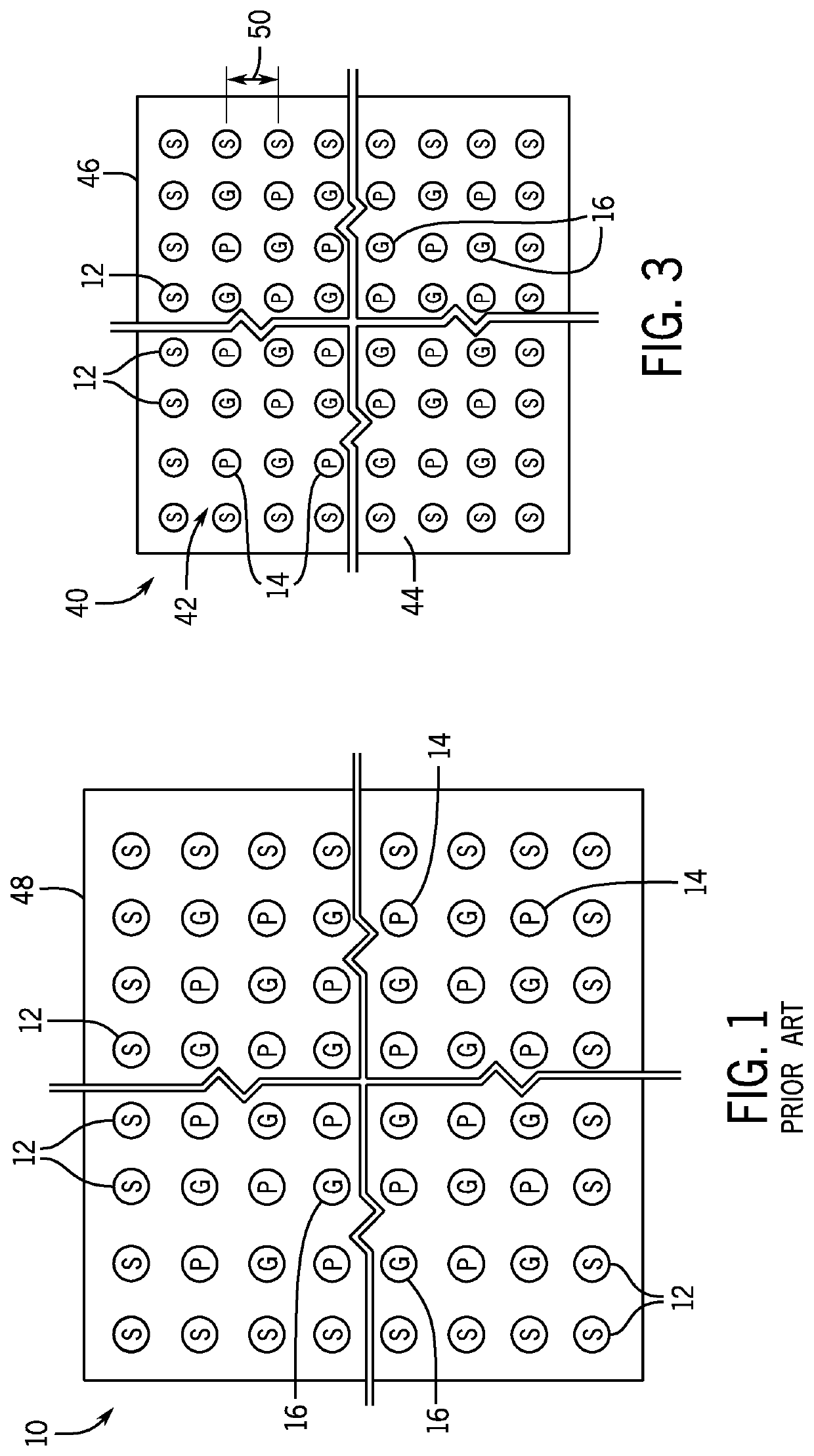
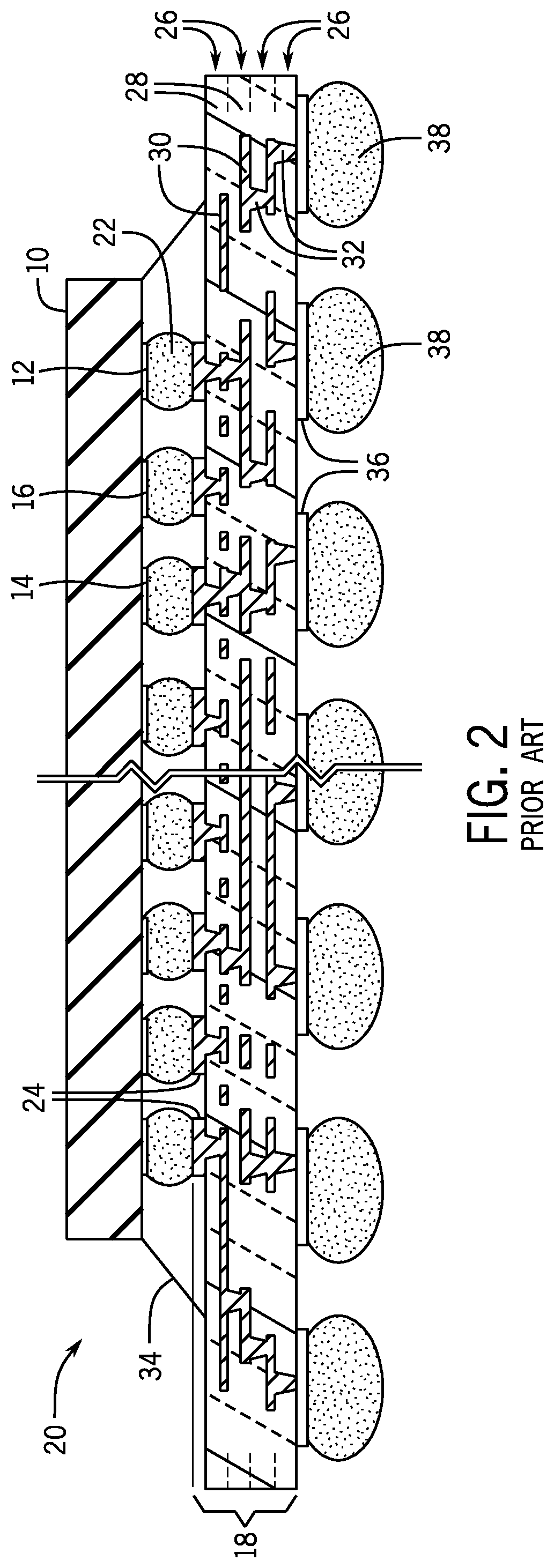
[0032]Embodiments of the present invention provide for semiconductor logic devices provided with a reconfiguration layer that includes bussed connections to power and ground input / output (I / O) pads and enables improved electrical performance, improved packaging yields, and reduced chip costs. The bussed power and ground terminals provide the capability to shrink the overall size of the semiconductor logic device while maintaining or improving power and ground signal delivery. Interconnect packaging structures are also disclosed herein that provide for an embedded chip module that incorporates these reconfigured and improved semiconductor logic devices with acceptable yield losses.

[0033]As used herein, the term “semiconductor logic device” refers to a semiconductor component, integrated circuit, device, die or chip that processes digital data in order to control the operation of electronic systems. Semiconductor logic devices are constructed from small electronic circuits called logi...


PUM

PropertyMeasurementUnit
feature sizesaaaaaaaaaa
sizeaaaaaaaaaa
sizeaaaaaaaaaa

Abstract

A reconfigured semiconductor logic device includes a semiconductor logic device comprising a plurality of input / output (I / O) pads formed on an active surface thereof and a redistribution layer. The redistribution layer comprises an insulating layer formed atop the active surface of the semiconductor logic device such that the insulating layer does not extend beyond an outer perimeter of the active surface and a patterned conductive wiring layer positioned above the insulating layer. The patterned conductive wiring layer includes a plurality of terminal buses formed on a top surface of the insulating layer. Each terminal bus of the plurality of terminal buses is electrically coupled to multiple I / O pads of the plurality of I / O pads through vias formed in the insulating layer.

Description

BACKGROUND OF THE INVENTION[0001]Embodiments of the invention relate generally to semiconductor logic devices and structures and methods for packaging semiconductor logic devices within embedded chip packages.[0002]High performance, high pin count semiconductor logic devices or chips have hundreds or thousands of input / output (“I / O”) pads for signals, power, and ground. FIG. 1 depicts an exemplary prior art semiconductor logic device 10 with signal I / O pads 12, power I / O pads 14, and ground I / O pads 16 arranged for flip chip solder bump attach. As shown, I / O pads 12, 14, 16 have the same pad size or diameter and are arranged in a uniform array on a grid of uniform x-axis pitch and y-axis pitch distributed over the whole surface of the device 10. A skilled artisan will recognize that a typical complex semiconductor logic device such as a microprocessor, applications processor, or graphics processor would have many more I / O pads than illustrated in FIG. 1. As such, semiconductor logic...

Claims


Application Information

Patent Timeline
Patent Type & Authority Patents(United States)
IPC IPC(8): H01L23/00H01L25/00H01L21/56H01L23/528H01L25/10H01L23/31H01L23/50H01L25/065
CPCH01L25/105H01L24/06H01L23/50H01L24/24H01L24/13H01L21/565H01L23/5286H01L23/3121H01L25/0655H01L24/20H01L24/19H01L25/50H01L2225/1058H01L2224/06131H01L2224/24137H01L2225/1041H01L2924/20641H01L2224/0401H01L2224/211H01L2924/1431H01L2924/37001H01L2224/02379H01L2224/0231H01L2924/2064H01L2224/13024H01L23/5389H01L2224/73204H01L21/568H01L23/3128H01L2924/00014H01L2924/181H01L2924/1433H01L2924/1434H01L23/49816H01L23/5384H01L23/5383H01L23/5386H01L2224/92144H01L2924/15331H01L2224/32225H01L24/82H01L2924/00012H01L2224/16225H01L2224/13099
Inventor FILLION, RAYMOND ALBERTNAGARKAR, KAUSTUBH RAVINDRA
Owner GENERAL ELECTRIC CO
Features
  • R&D
  • Intellectual Property
  • Life Sciences
  • Materials
  • Tech Scout
  • Unparalleled Data Quality
  • Higher Quality Content
  • 60% Fewer Hallucinations
Learn More