

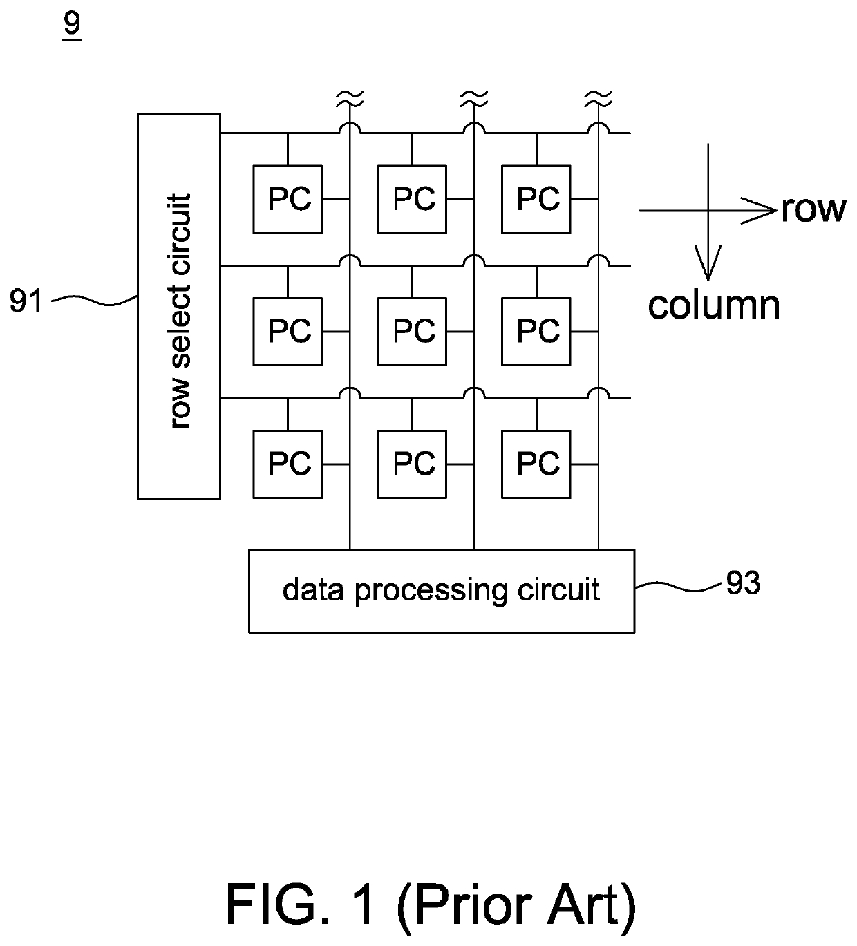
Image sensor capable of averaging pixel data
a technology of image sensor and pixel data, applied in the field of image sensor, can solve problems such as the inability to reduce the system power consumption, and achieve the effect of improving the signal-to-noise ratio (snr)
- Summary
- Abstract
- Description
- Claims
- Application Information
AI Technical Summary
Benefits of technology
Problems solved by technology
Method used
Image

Examples
first embodiment
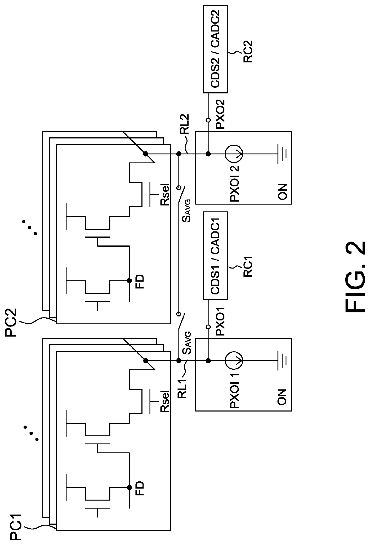
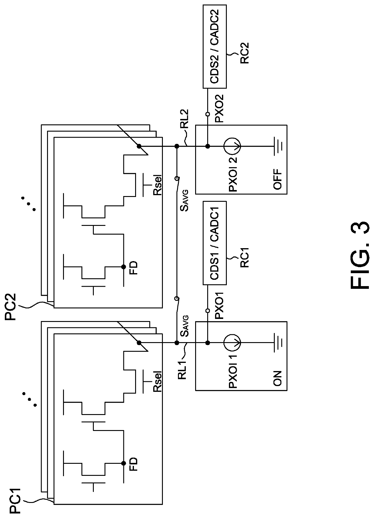
[0025]Referring to FIGS. 2 and 3, they are operational schematic diagrams of a first mode and a second mode, respectively, of an image sensor according to the present disclosure, wherein the first mode is a normal mode such as a photographing mode, an image preview mode or a face recognition mode; the second mode is, for example, a sleep mode or a low power mode. In the second mode, pixel data is averaged by at least one average switch, and a part of components of the readout circuit is shut down.
[0026]The image sensor of the present disclosure includes a pixel array, a drive circuit (not shown) and readout circuits. The pixel array of the present disclosure includes a plurality of pixel circuits arranged in a matrix, e.g., arranged as a plurality of pixel circuit columns and a plurality of pixel circuit rows. For example, FIG. 2 shows a first pixel circuit PC1 and a second pixel circuit PC2 in two columns of the plurality of pixel circuit columns of the pixel array. Preferably, the...
second embodiment
[0041]The image sensor in FIG. 5 also includes the first pixel circuit PC1, the second pixel circuit PC2, the first readout line RL1 and the second readout line RL2 as described above, and thus details thereof are not repeated herein. The image sensor of the second embodiment further includes a first column analog-to-digital converter CADC1 connected to all pixel circuits in the same column (e.g., the first column, but not limited to) as the first pixel circuit PC1 via the first readout line RL1, and includes a second column analog-to-digital converter CADC2 connected to all pixel circuits in the same column (e.g., the second column, but not limited to) as the second pixel circuit PC2 via the second readout line RL2.
[0042]The CADC1 includes a first comparator 411, a first detected signal sample capacitor C11 and a first reference signal sample capacitor C12. The first detected signal sample capacitor C11 is coupled to one input terminal (e.g., inverting input) of the first comparato...
third embodiment
[0051]The image sensor of the third embodiment further includes a first storing circuit 611, a second storing circuit 612, a first voltage buffer 631 and a second voltage buffer 632. The first storing circuit 611 is coupled between the first readout line RL1 (e.g., output terminal PXO1) and the CADC1 (e.g., node IN1), and used to store pixel data of the first pixel circuit PC1 before the averaging. The second storing circuit 612 is coupled between the second readout line RL2 (e.g., output terminal PXO2) and the CADC2 (e.g., node IN2), and used to store pixel data of the second pixel circuit PC2 before the averaging.
[0052]The first voltage buffer 631 is coupled between the first storing circuit 611 and the CADC1 for nondestructively buffer the voltage (i.e. pixel data) stored in the first storing circuit 611 to the first detected signal sample capacitor C11. The second voltage buffer 632 is coupled between the second storing circuit 612 and the CADC2 for nondestructively buffer the v...
PUM
 Abstract
Description
Claims
Application Information