Electronic device

a technology of electronic devices and components, applied in the direction of individually energised antenna arrays, resonant antennas, printed circuit non-printed electric components association, etc., can solve problems such as wrinkles or sinking deformation, and achieve efficient signal transmission and reception, enhance rigidity, and increase the residual rate of copper foil

Active Publication Date: 2020-05-19
LG ELECTRONICS INC
View PDF8 Cites 2 Cited by
  • Summary
  • Abstract
  • Description
  • Claims
  • Application Information

AI Technical Summary

Benefits of technology

[0008]An object of the present disclosure is to solve the foregoing problems and other problems, and provide a structure of an electronic device capable of ensuring sufficient antenna performance at operating frequency as well as preventing deterioration in quality of a patch antenna applied to a circuit board composed of a plurality of layers.
[0009]Furthermore, another object of the present disclosure is to provide a structure of an electronic device capable of performing physical reinforcement of a circuit board mounted with a patch antenna and restricting signal interference between a plurality of patch antennas.
[0015]The electronic device having the above structure may include a first EBG structure and a second EBG structure, thereby preventing operating frequency signals from interfering with each other between adjacent patch antennas as well as allowing efficient signal transmission and reception.
[0016]In addition, the first EBG structure and the second EBG structure may be arranged symmetrically with respect to a core layer inside the circuit board to increase a copper foil residual rate on a conductive layer where the EBG structure is positioned so as to enhance rigidity, thereby minimizing deformation due to high pressure or temperature applied to the circuit board.

Problems solved by technology

The circuit board having such a structure may be deformed by an externally applied pressure or impact or high temperature, and there is a problem that wrinkle or sinking deformation may occur at a portion where the conductive material is removed.

Method used


Image

  • Electronic device
  • Electronic device
  • Electronic device

Examples


Embodiment Construction

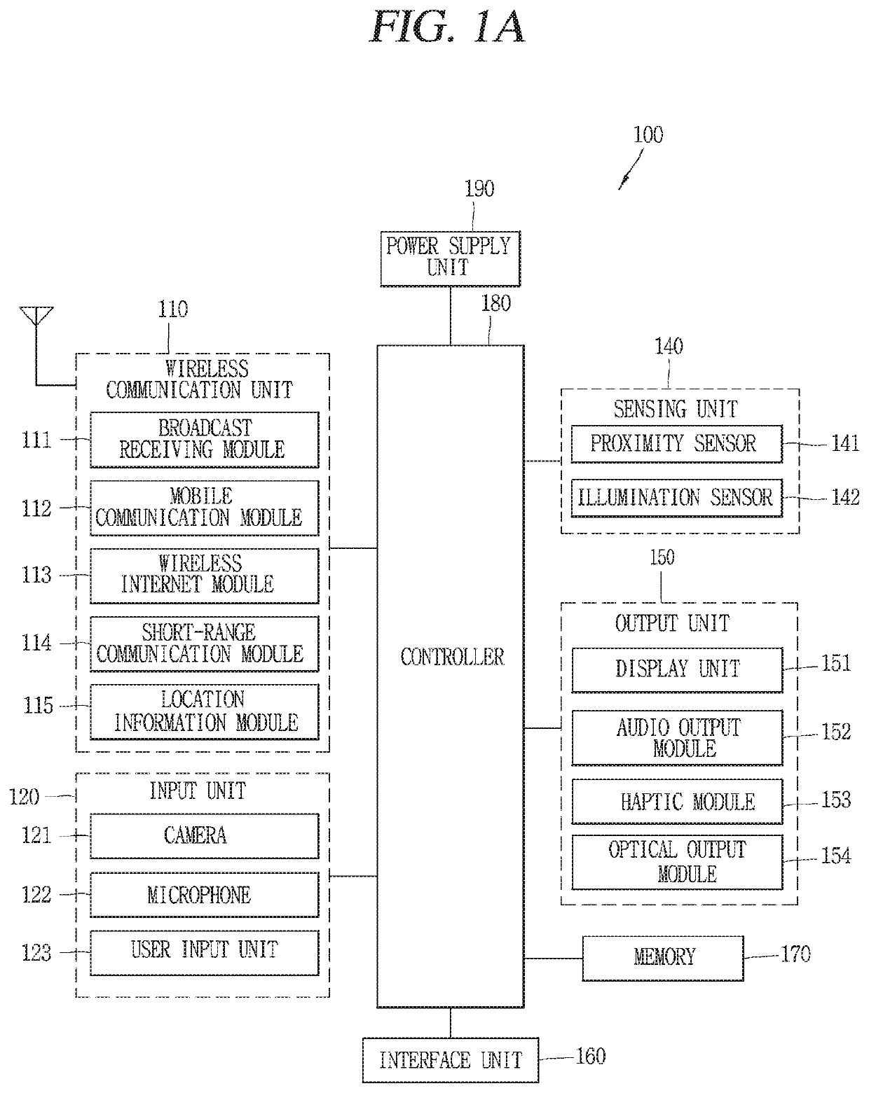
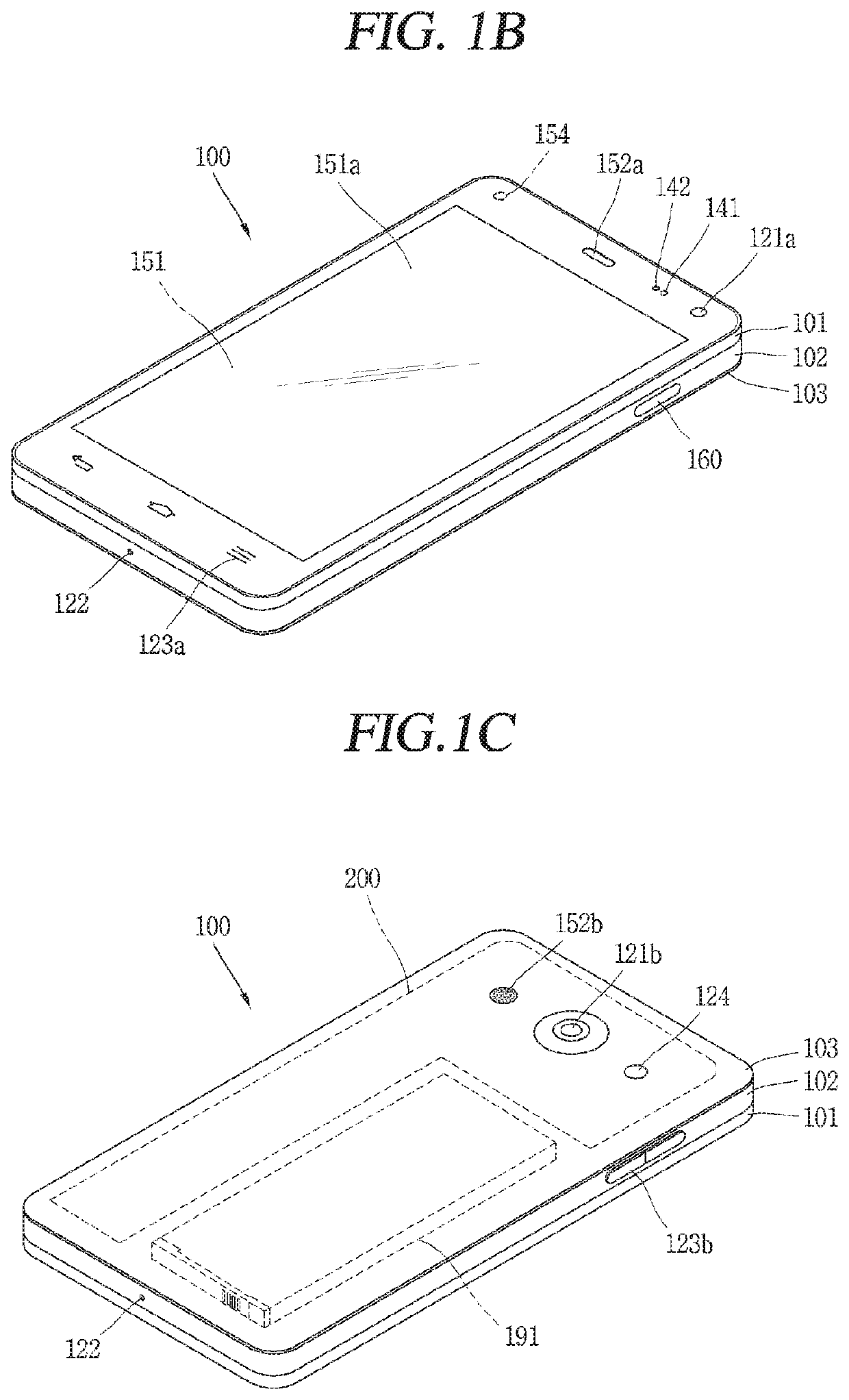
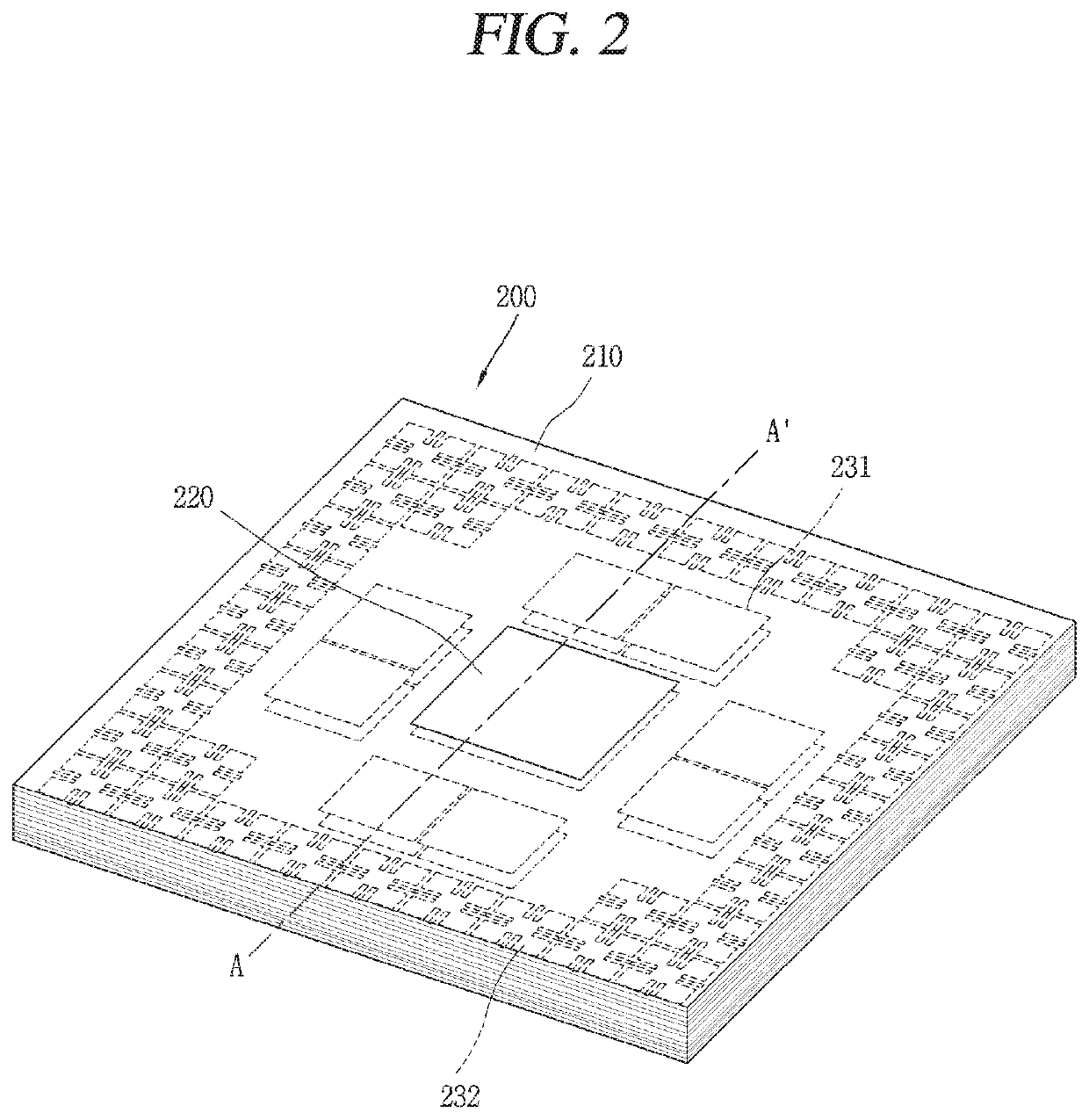
[0037]Hereinafter, preferred embodiments of the present disclosure will be described in detail with reference to the accompanying drawings, and the same or similar elements are designated with the same numeral references regardless of the numerals in the drawings and their redundant description will be omitted. A suffix “module” or “unit” used for constituent elements disclosed in the following description is merely intended for easy description of the specification, and the suffix itself does not give any special meaning or function. In describing the present disclosure, if a detailed explanation for a related known function or construction is considered to unnecessarily divert the gist of the present disclosure, such explanation has been omitted but would be understood by those skilled in the art. The accompanying drawings are used to help easily understand the technical idea of the present disclosure and it should be understood that the idea of the present disclosure is not limit...


PUM

PropertyMeasurementUnit
frequenciesaaaaaaaaaa

Abstract

The present disclosure relates to an electronic device, and the electronic device may include a circuit board provided within a main body of the electronic device, on which a conductive layer made of a conductive material and a dielectric layer made of an insulating material are alternately laminated; at least one or more patch antennas disposed on the circuit board; a core layer located at a central portion inside the circuit board, and configured with any one of the dielectric layers; a ground layer disposed below the core layer; and an EBG structure located inside the circuit board in a symmetrical shape at the top and bottom with respect to the core layer, and the EBG structure restricts operating frequency signals radiated from the respective patch antennas from being interfered with each other.

Description

CROSS-REFERENCE TO RELATED APPLICATIONS[0001]Pursuant to 35 U.S.C. § 119, this application claims the benefit of earlier filing date and right of priority to U.S. Provisional Application No. 62 / 564,222, filed on Sep. 27, 2017, and also claims the benefit of Korean Application No. 10-2018-0020712, filed on Feb. 21, 2018, the contents of which are all incorporated by reference herein in their entirety.BACKGROUND OF THE INVENTION1. Field of the Invention[0002]The present disclosure relates to an electronic device including a circuit board mounted with an EBG structure.2. Description of the Related Art[0003]Electronic devices may be implemented in the form of a multimedia device having a combination of functions such as capturing still or moving images, playing music or video files, gaming, and receiving broadcast and the like using various electronic components provided in a main body thereof.[0004]Furthermore, in recent years, as the multimedia function of such an electronic device is...

Claims


Application Information

Patent Timeline
Patent Type & Authority Patents(United States)
IPC IPC(8): H01Q1/48H05K1/02H01Q9/04H01Q21/06H05K1/18H05K1/11H01Q1/52
CPCH01Q1/521H05K1/0236H05K1/115H05K1/181H01Q1/48H01Q21/065H05K1/0271H01Q9/045H05K1/0298H05K2201/10098H01Q15/006H01Q9/0457H01Q9/0414
Inventor WOO, SEUNGMIN
Owner LG ELECTRONICS INC
Why Eureka
Try Eureka