Multi-wafer stacking structure and fabrication method thereof

a stacking structure and multi-wafer technology, applied in the direction of electrical equipment, semiconductor devices, semiconductor/solid-state device details, etc., can solve the problems of reducing signal transmission speed, high cost, and reducing the thickness of multi-wafer stacking, so as to reduce the overall device thickness, reduce the thickness of the overall device, and increase the density of the packag

Active Publication Date: 2020-06-30
WUHAN XINXIN SEMICON MFG CO LTD
View PDF13 Cites 0 Cited by
  • Summary
  • Abstract
  • Description
  • Claims
  • Application Information

AI Technical Summary

Benefits of technology

[0005]The present invention is directed to a multi-wafer stacking structure, intended to reduce the overall thickness after multi-wafer stacking.
[0006]The present invention is also directed to no need of leads, thereby improving the signal transmission speed and reducing the power loss.
[0029]In the multi-wafer stacking structure and method provided by the present invention, a first interconnection layer is electrically connected to a first metal layer and a second metal layer via a first opening, a second interconnection layer is electrically connected to the first interconnection layer via a second opening, a third interconnection layer is electrically connected to a third metal layer via a third opening, and the second interconnection layer is in contact with the third interconnection layer. It is unnecessary to reserve a bonding lead space between wafers, a silicon substrate is eliminated, and the multi-wafer stacking thickness is reduced while multi-wafer interconnection is realized, so that the overall device thickness is reduced after multi-wafer stacked package, the package density is increased, and the requirements for increasingly thinning semiconductor products are met. Moreover, there is no need of leads for the multi-wafer stacking structure, so as to eliminate design processing of a silicon substrate and a plurality of shared bonding pads on the silicon substrate, thereby facilitating cost reduction and process simplification. In addition, the second interconnection layer is in contact with the third interconnection layer to shorten an interconnection distance between wafers, thus reducing the parasitic capacitance and the power loss, and improving the transmission speed.

Problems solved by technology

But the inventor finds that some problems exist in the traditional multi-wafer lead interconnection manner.
In addition, gold wires are generally adopted as the leads, and therefore, the cost is relatively high.
Moreover, the leads result in a relatively long interconnection line, which reduces the signal transmission speed and increases the power loss.
Furthermore the silicon substrate cannot be adapted to the requirement on more and more sharing bonding pads for high-density development of the multi-wafer stacking.

Method used


Image

  • Multi-wafer stacking structure and fabrication method thereof
  • Multi-wafer stacking structure and fabrication method thereof
  • Multi-wafer stacking structure and fabrication method thereof

Examples


Embodiment Construction

[0054]The multi-wafer stacking structure and method proposed by the present invention are further described in detail below with reference to the accompanying drawings and specific embodiments. The advantages and features of the present invention will be clearer according to the following description. It is to be noted that the accompanying drawings are in a very simple form and in a non-accurate proportion, and are only for the purpose of conveniently and clearly supporting the description of the present invention.

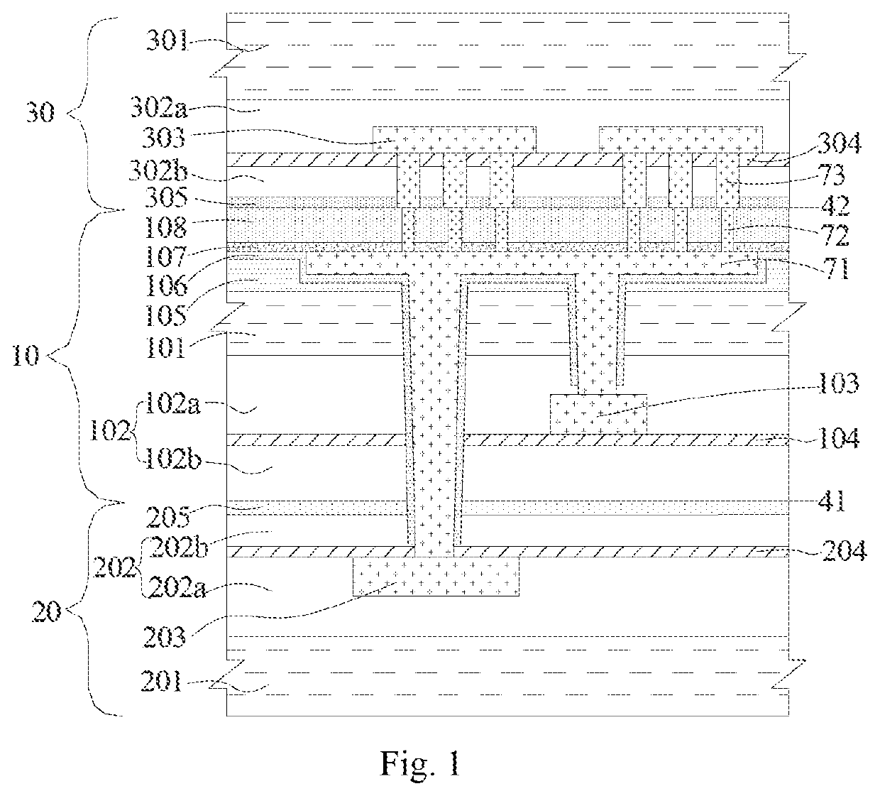
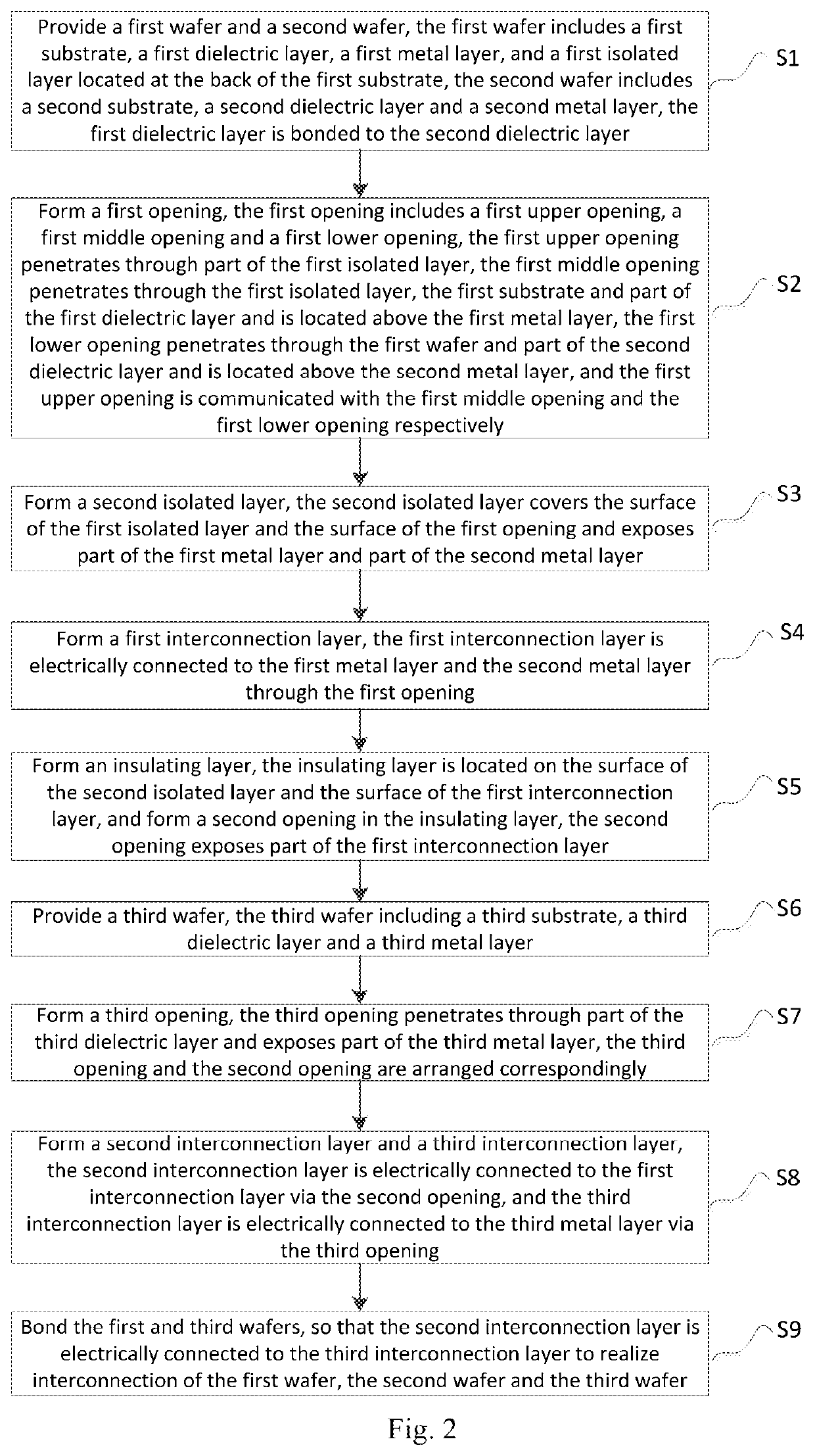
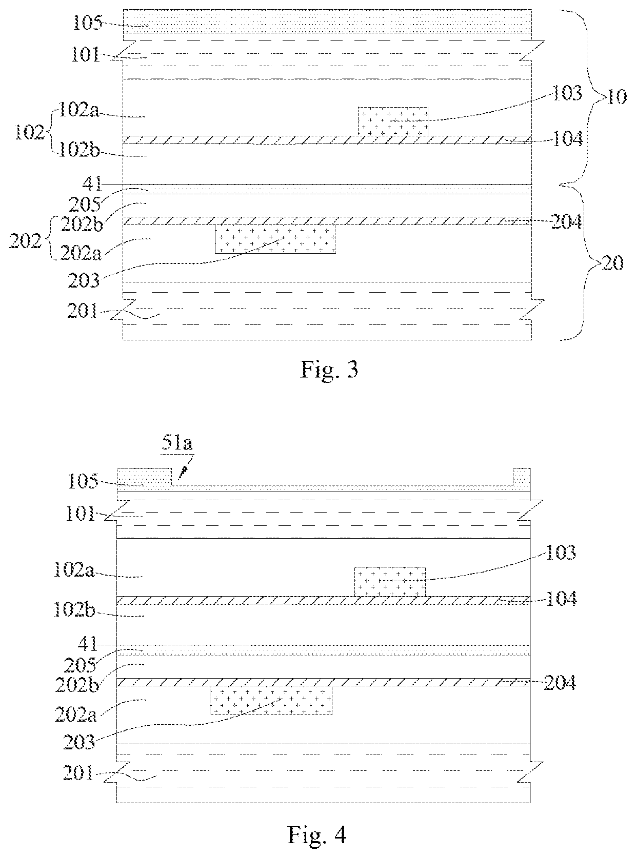
[0055]The multi-wafer stacking structure provided by the embodiment of the present invention is introduced in detail below as shown in FIG. 1, FIG. 7, FIG. 12 and FIG. 13. A multi-wafer stacking structure includes:

[0056]a first wafer 10, wherein the first wafer 10 includes a first substrate 101, a first dielectric layer 102 located on the first substrate 101, a first metal layer 103 embedded in the first dielectric layer 102, and a first isolated layer 105 located at the ...


PUM

PropertyMeasurementUnit
thicknessaaaaaaaaaa
densityaaaaaaaaaa
speedaaaaaaaaaa

Abstract

A multi-wafer stacking structure and fabrication method are disclosed. In the multi-wafer stacking structure, a first interconnection layer is electrically connected to a second metal layer and a first metal layer via a first opening, a second interconnection layer is electrically connected to the first interconnection layer via a second opening, a third interconnection layer is electrically connected to a third metal layer via a third opening, and the second interconnection layer is electrically connected to the third interconnection layer. It is unnecessary to reserve a bonding lead space between wafers, a silicon substrate is eliminated, and the multi-wafer stacking thickness is reduced while multi-wafer interconnection is realized, so that the overall device thickness is reduced after multi-wafer stacked package. Moreover, there is no need of leads, so as to eliminate design processing of a silicon substrate and a plurality of shared bonding pads on the silicon substrate.

Description

CROSS-REFERENCE TO RELATED APPLICATION[0001]This application claims the priority of Chinese patent application number 201810990635.9, filed on Aug. 28, 2018, the entire contents of which are incorporated herein by reference.TECHNICAL FIELD[0002]The present invention belongs to the technical field of manufacturing of integrated circuits, and in particular, to a multi-wafer stacking structure and a fabrication method thereof.BACKGROUND[0003]Under the tendency of development of highly integrated semiconductors, after multi-wafer stacking, a manner of lead bonding is generally adopted to realize interconnection among multiple wafers. Specifically, multiple wafers are stacked along a vertical direction on a special silicon substrate. Each wafer has multiple bonding pads used for interconnection, a plurality of sharing bonding pads are arranged on the silicon substrate. One end of each of leads is bonded to a corresponding one of the bonding pads of the wafer in a pressure welding manner,...

Claims


Application Information

Patent Timeline
Patent Type & Authority Patents(United States)
IPC IPC(8): H01L21/76H01L25/00H01L23/00H01L25/065H01L23/48H01L21/768
CPCH01L21/76898H01L25/0657H01L24/80H01L24/08H01L23/481H01L25/50H01L2224/80896H01L2224/80895H01L2225/06524H01L2224/08146H01L2225/06544H01L23/5226H01L23/5283H01L21/76804H01L21/76816H01L23/367H01L27/0688H01L2224/9202H01L2224/82031H01L2224/82106H01L2224/24011H01L2224/24051H01L2224/24146H01L2224/09181H01L24/82H01L24/92H01L24/24H01L2224/80001H01L2224/82H01L2924/00014
Inventor ZHAO, CHANGLINZENG, TIAN
Owner WUHAN XINXIN SEMICON MFG CO LTD
Why Eureka
Try Eureka