Lead frame

a lead frame and sealing resin technology, applied in the field of lead frame, can solve the problems of frame reliability, poor adhesion of silver or silver alloy to sealing resin, and inability to use the technique, so as to improve productivity, reduce cost and working time, and increase adhesion to sealing resin.

Active Publication Date: 2020-09-01
CHANG WAH TECH
View PDF15 Cites 0 Cited by
  • Summary
  • Abstract
  • Description
  • Claims
  • Application Information

AI Technical Summary

Benefits of technology

[0016]According to the embodiment modes of the present invention, in a lead frame in which silver plating, as the outermost plating layer, is applied to the entire surface of the lead frame substrate, it is possible to stay the total thickness of plating layers including the silver plating layer to be small and to remarkably increase adhesion to the sealing resin, while reducing cost and working time, to improve productivity.

Problems solved by technology

Silver or an alloy containing silver, however, has poor adhesion to a sealing resin.
Therefore, such a lead frame involves a problem in reliability, for the sealing resin is easily peeled off the lead frame by shock or heat.
For this reason, it is unsuitable to use the technique of roughening the surface of a lead frame substrate made of a copper alloy into a roughened state having concavities and convexities by microetching process.
However, even if the plating layer made of a precious metal or a precious metal alloy is made thin, the adhesion to the resin cannot be improved.

Method used


Image

  • Lead frame
  • Lead frame
  • Lead frame

Examples


first embodiment

Mode

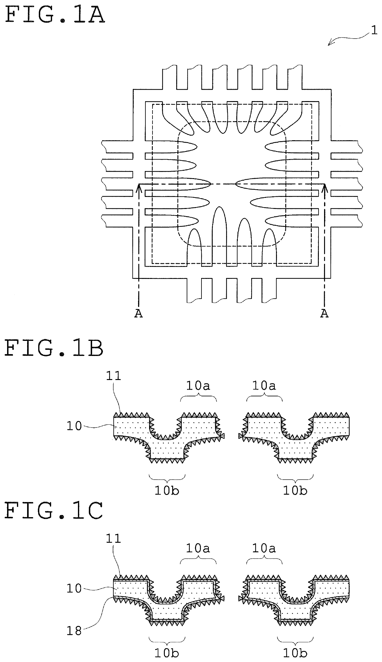
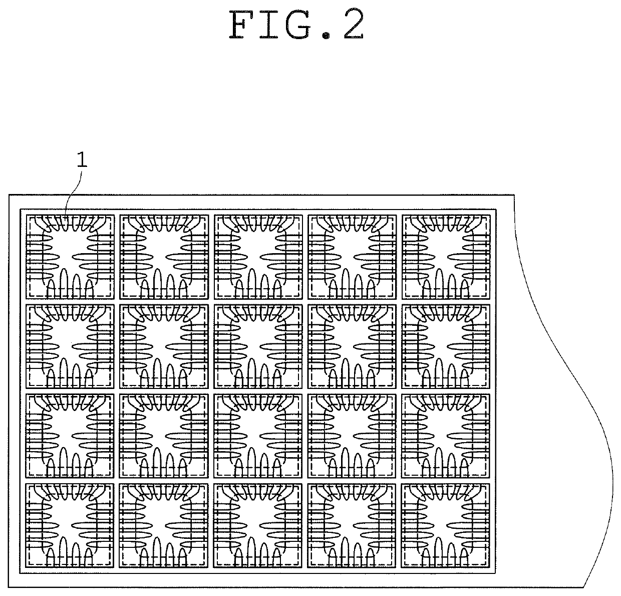
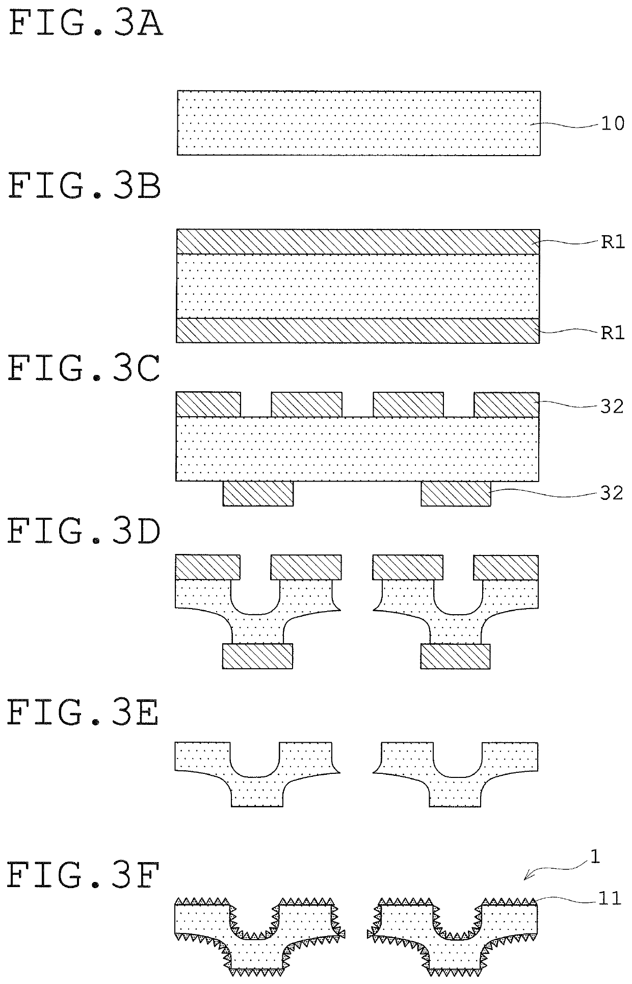
[0052]FIGS. 1A-1B are diagrams that show one example of a lead frame according to a first embodiment mode of the present invention, where FIG. 1A is a plan view and FIG. 1B is an explanatory diagram schematically showing the A-A cross section in FIG. 1A. FIG. 1C is a diagram that shows a modification of the lead frame of the first embodiment mode shown in FIGS. 1A-1B. FIG. 2 is a plan view that shows one example of lead frames arrayed in multiple rows according to the first embodiment mode of the present invention. FIGS. 3A-3F are explanatory diagrams that show an exemplary manufacturing procedure of a lead frame for mounting a semiconductor element thereon according to the first embodiment mode of the present invention. FIGS. 4A-4E are explanatory diagrams that show an exemplary manufacturing procedure of a semiconductor package using the lead frame for mounting a semiconductor element thereon according to the first embodiment mode of the present invention.

[0053]As shown in FIG...

second embodiment

Mode

[0082]FIGS. 5A-5B are diagrams that show one example of a lead frame according to a second embodiment mode of the present invention, where FIG. 5A is a plan view and FIG. 5B is an explanatory diagram schematically showing a B-B cross section in FIG. 5A. FIG. 6 is a plan view that shows one example of lead frames arrayed in multiple rows according to the second embodiment mode of the present invention. FIGS. 7A-7F are explanatory diagrams that show an exemplary manufacturing procedure for a lead frame for mounting a semiconductor element thereon according to the second embodiment mode of the present invention. FIGS. 8A-8E are explanatory diagrams that show an exemplary manufacturing procedure for a semiconductor package using the lead frame for mounting a semiconductor element thereon according to the second embodiment mode of the present invention.

[0083]As shown in FIGS. 5A-5B, a lead frame 1′ of this embodiment mode includes a pad portion 10c for mounting a semiconductor elemen...

embodied example 1

[0103]A lead frame of Embodied Example 1 is an exemplary lead frame in which the roughened silver plating layer 11 is formed directly on the entire surface of the lead frame substrate 10 without an undercoat layer between.

[0104]In Embodied Example 1, a strip copper material having a thickness of 0.2 mm and a width of 180 mm was prepared as the lead frame substrate 10 (See FIG. 3A). Resist layers R1 with a thickness of 25 μm were formed on both surfaces of the copper material (See FIG. 3B) and was developed after exposure upon use of glass masks carrying predetermined patterns, to form etching resist masks 32 (See FIG. 3C). Then, etching treatment was made (See FIG. 3D) and the etching resist mask 32 were removed, to form a lead frame having a predetermined shape (See FIG. 3E).

[0105]The entire surface of the metal plate 10, which had been shaped into the predetermined lead frame shape, was subjected to pretreatment with alkali and acid, and then was electroplated in the following man...


PUM

PropertyMeasurementUnit
average crystal grain diameteraaaaaaaaaa
diameteraaaaaaaaaa
diameteraaaaaaaaaa

Abstract

A lead frame includes, as an outermost plating layer, a roughened silver plating layer having acicular projections and covering the entire surface of a lead frame substrate made of a copper-based material. The roughened silver plating layer has a crystal structure in which the crystal direction <101> occupies a largest proportion among the crystal directions <001>, <111>, and <101>. The lead frame can be manufactured with improved productivity owing to reduction in cost and operation time, and achieves remarkably high adhesion to sealing resin while keeping the total thickness of plating layers including the silver plating layer to be thin.

Description

CROSS-REFERENCE TO RELATED PATENT APPLICATIONS[0001]This application claims the benefit of Japanese Patent Application No. 2019-055683 filed in Japan on Mar. 22, 2019, the contents of which are incorporated herein by reference.BACKGROUND OF THE INVENTION1) Field of the Invention[0002]The present invention relates to a lead frame for a semiconductor in which silver plating, as outermost plating, is applied to the entire surface of a lead frame substrate.2) Description of Related Art[0003]One of devices for mounting a semiconductor element thereon is a lead frame. Conventionally, often used are lead frames in which silver plating, as outermost plating, is applied to the entirety or a part of the surface of a lead frame substrate. Silver or an alloy containing silver, however, has poor adhesion to a sealing resin. Therefore, such a lead frame involves a problem in reliability, for the sealing resin is easily peeled off the lead frame by shock or heat.[0004]To solve this problem, there ...

Claims


Application Information

Patent Timeline
Patent Type & Authority Patents(United States)
IPC IPC(8): H01L23/495H01L21/56H01L23/00H01L23/31H01L21/48
CPCH01L23/49582H01L21/4828H01L24/73H01L24/16H01L21/56H01L24/32H01L23/3121H01L24/48H01L23/49541H01L2224/73265H01L2224/48106H01L2224/16245H01L2224/48245H01L2224/32245H01L2224/48091H01L23/49517H01L23/495H01L2224/48247H01L2224/97H01L23/49548H01L23/3107H01L23/3142H01L21/561H01L2224/81385H01L2224/81439H01L2224/81455H01L2224/81444H01L2224/81464H01L2224/131H01L2224/83385H01L2224/83439H01L2224/83444H01L2224/83455H01L2224/83464H01L2224/85464H01L2224/85455H01L2224/85444H01L2224/85439H01L2224/85385H01L24/83H01L24/85H01L24/81H01L24/13H01L2924/00014H01L2924/014H01L2224/81H01L2224/83H01L2224/85H01L2924/00012H01L21/4821
Inventor HISHIKI, KAORUOTAKI, KEIICHISASAKI, HIDEHIKOTOMEOKA, KOTARO
Owner CHANG WAH TECH
Why Eureka
Try Eureka