Gate driver and semiconductor module

a technology of gate driver and semiconductor module, which is applied in the direction of power conversion system, pulse technique, electronic switching, etc., can solve the problems of high design load, inability to secure desired voltage and current, and increased cost or improvement of power supply quality, etc., and achieve the effect of reducing the design load

Active Publication Date: 2020-09-22
MITSUBISHI ELECTRIC CORP
View PDF6 Cites 5 Cited by
  • Summary
  • Abstract
  • Description
  • Claims
  • Application Information

AI Technical Summary

Benefits of technology

[0005]Provided is a gate driver capable of reducing a design load and ensuring a desired voltage and current without increasing the maximum rating of the input power supply voltage of the gate driver.
[0007]According to the above gate driver, the offset voltage is applied to the source of the transistor in accordance with the timing of turning off the gate of the transistor, and the second potential is switched to be applied to the source of the transistor in accordance with the timing of turning on the gate. Therefore, even for a transistor having a low threshold voltage, it is not necessary to increase the maximum rating of the input power supply voltage of the gate driver. Also, a design load can be reduced and a desired voltage and current can be secured.

Problems solved by technology

For this reason, increase in the maximum rating of the input power supply voltage of the gate driver or reduction in the variation margin of the input power supply voltage is required, accordingly, there have been problems in that cost is increased or improvement of the quality of the power supply is required, which leads to a high design load.
However, with such power source generation, there has been a problem in that desired voltage and current could not be secured.

Method used


Image

  • Gate driver and semiconductor module
  • Gate driver and semiconductor module
  • Gate driver and semiconductor module

Examples


embodiment 1

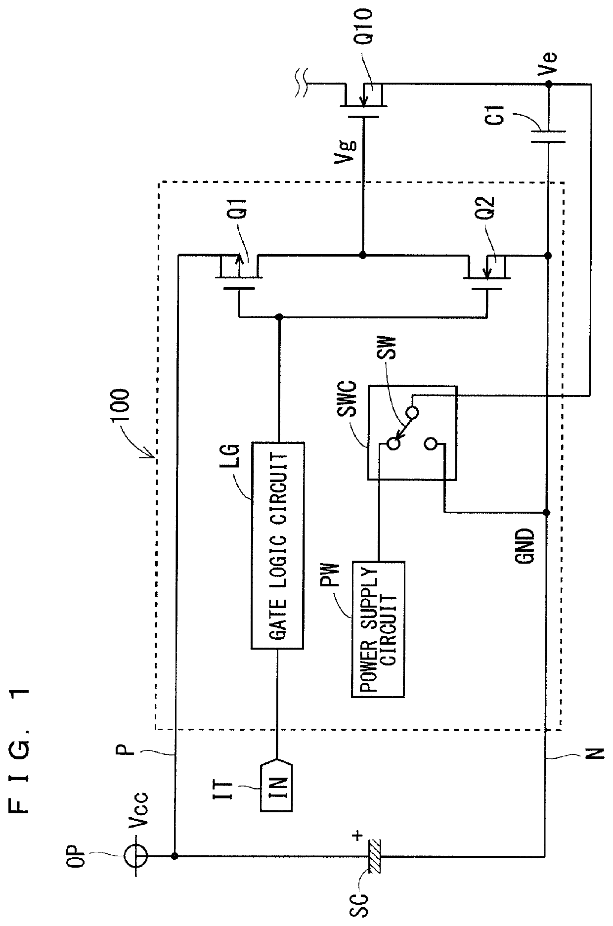
[0016]FIG. 1 is a circuit diagram illustrating a configuration of a gate driver according to Embodiment 1 of the present invention. As illustrated in FIG. 1, the gate driver 100 is a gate driver that drives an n-channel MOS transistor Q10 that is a power device, and is configured as an integrated circuit (IC).

[0017]The gate driver 100 includes a power supply line P (first power supply line) to which a voltage Vcc (first potential) is supplied from a power supply terminal OP, and a p-channel type MOS transistor Q1 (first transistor) and an n-channel type transistor Q2 (second transistor) connected in series with the ground line N (second power supply line) of the ground potential (second potential). The MOS transistors Q1 and Q2 operate in a complementary manner, and the connection node between the MOS transistor Q1 and the MOS transistor Q2 serves as an output node of the gate driver 100, from which a gate signal is output and the signal is input to the gate of the MOS transistor Q1...

embodiment 2

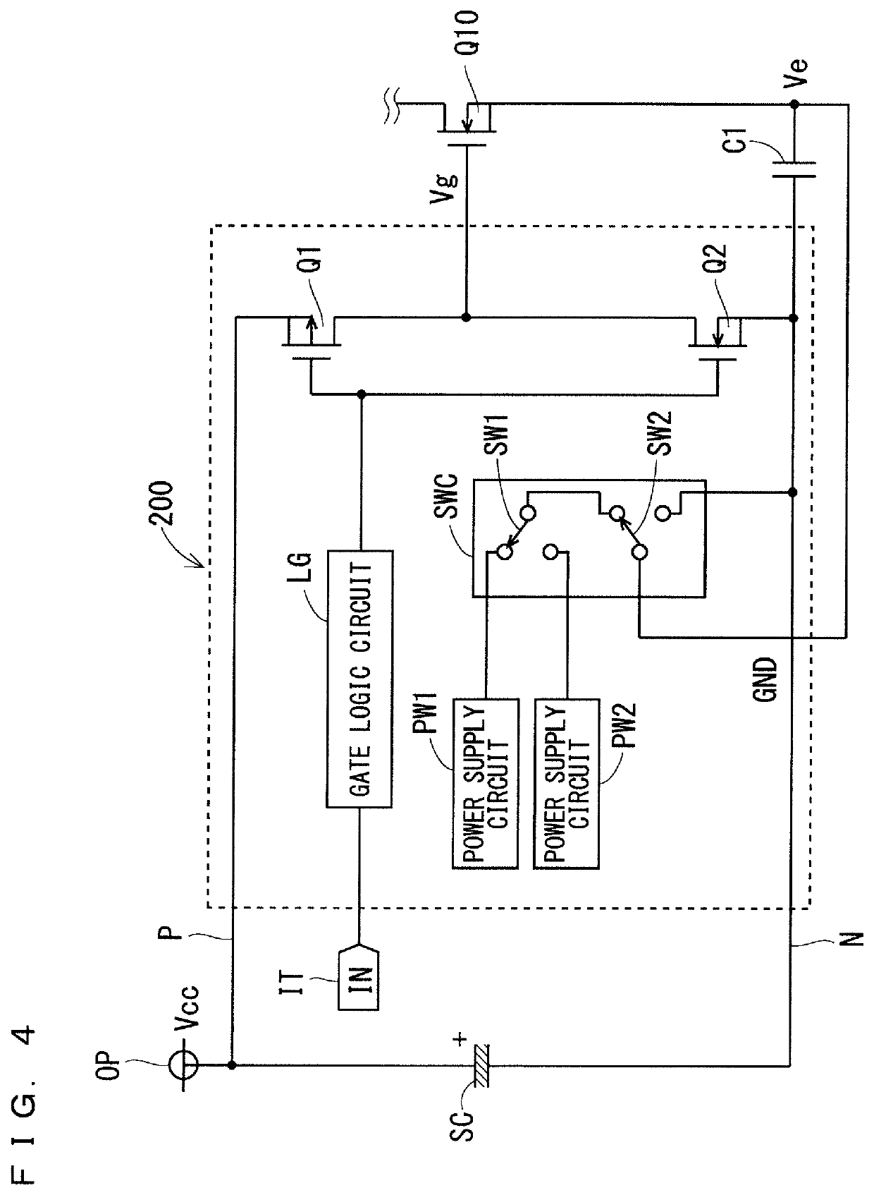
[0039]FIG. 4 is a circuit diagram illustrating a configuration of a gate driver 200 according to Embodiment 2 of the present invention. It should be noted that, in FIG. 4, the same components as those of the gate driver 100 described with reference to FIG. 1 are denoted with the same reference numerals, and overlapping descriptions are omitted.

[0040]As illustrated in FIG. 4, the gate driver 200 includes power supply circuits PW1 and PW2 and a switching circuit SWC for switching output destinations of the power supply circuits PW1 and PW2. The power supply circuits PW1 and PW2 are negative bias power supplies, and each output is connected to two nodes of the switch SW1 in the switching circuit SWC, respectively.

[0041]The switches SW1 and SW2 switch the outputs of power supply circuits PW1 and PW2 to connect either to the source of MOS transistor Q10 or to ground (GND). The switching circuit SWC controls the switch SW1 to switch from the output of the power supply circuit PW1 to the o...

embodiment 3

[0047]The gate driver 100 and the gate driver 200 of Embodiments 1 and 2 described above can be mounted on a semiconductor module as a driver IC.

[0048]FIG. 6 is a partial plan view illustrating an inner configuration of a semiconductor module 1000 according to Embodiment 3 of the present invention. As illustrated in FIG. 6, the semiconductor module 1000 is a module packaged with the MOS transistor Q10 using the gate driver 100 or the gate driver 200 as the gate driver GD. Note that in FIG. 6, the sealing resin and the like are not illustrated for convenience, but a package region PG sealed with the sealing resin is surrounded by a broken line, and outside this region is outside the module.

[0049]As illustrated in FIG. 6, the semiconductor module 1000 is a module in which three MOS transistors Q10 are packaged. The three MOS transistors Q10 are modules that are connected in parallel to each other at a portion that is not illustrated in the drawing to obtain a large output current. Not...


PUM


Abstract

A gate driver includes a first transistor and a second transistor connected in series between a first and a second power supply line, connection nodes thereof are output nodes of the gate driver, the first and second transistors being configured to operate in a complementary manner, a power supply circuit for applying an offset voltage to a source of the transistor, and a switching circuit for performing switching control to apply the offset voltage output from the power supply circuit to the source of the transistor or to apply the second potential to the source of the transistor. The switching circuit is configured to switch so as to apply the offset voltage to the source of the transistor in accordance with a timing of turning off the gate of the transistor and to apply the second potential to the source in accordance with a timing of turning on the gate.

Description

BACKGROUND OF THE INVENTIONField of the Invention[0001]The present invention relates to a gate driver, and more particularly to a gate driver for driving a gate of a transistor having a low gate threshold voltage.Description of the Background Art[0002]A case where the threshold voltage of the transistor is 0 V or less, or is a voltage at a level of lowness where malfunction may be caused due to noise or the like is concerned even if the threshold voltage is 0V or more, the malfunction that the transistor is turned on during the off-state is suppressed by applying a negative bias to the transistor source to increase the threshold voltage substantially.[0003]When the threshold voltage becomes substantially high in this manner, the gate driver needs to output a voltage obtained by adding a negative bias voltage to the gate voltage necessary for the gate drive in order to turn on the transistor. For this reason, increase in the maximum rating of the input power supply voltage of the gat...

Claims


Application Information

Patent Timeline
Patent Type & Authority Patents(United States)
IPC IPC(8): H03K17/687H02M1/08
CPCH02M1/08H03K17/6871H03K17/687H03K2217/0081H03K2217/0054H03K2017/066H03K17/163
Inventor SAKAI, SHINJI
Owner MITSUBISHI ELECTRIC CORP
Why Eureka
Try Eureka