Nitride semiconductor device

a semiconductor and nitride technology, applied in the direction of semiconductor devices, basic electric elements, electrical appliances, etc., can solve the problem of difficult to adopt a general vertical transistor package, and achieve the effect of low resistan

Active Publication Date: 2020-10-13
ROHM CO LTD
View PDF7 Cites 0 Cited by
  • Summary
  • Abstract
  • Description
  • Claims
  • Application Information

AI Technical Summary

Benefits of technology

[0012]According to the embodiments of the present disclosure, a low resistance region is formed in the second nitride semiconductor layer directly under a back-surface-drawing target electrode.
[0018]According to the embodiments of the present disclosure, a low resistance region is formed in the second nitride semiconductor layer directly under the drain electrode.

Problems solved by technology

Therefore, it is difficult to adopt a general vertical transistor package.

Method used


Image

  • Nitride semiconductor device
  • Nitride semiconductor device
  • Nitride semiconductor device

Examples


first embodiment

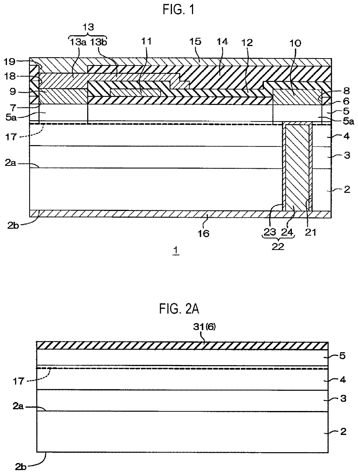
[0071]FIG. 1 is a sectional view for explaining a configuration of a nitride semiconductor device according to the present disclosure.

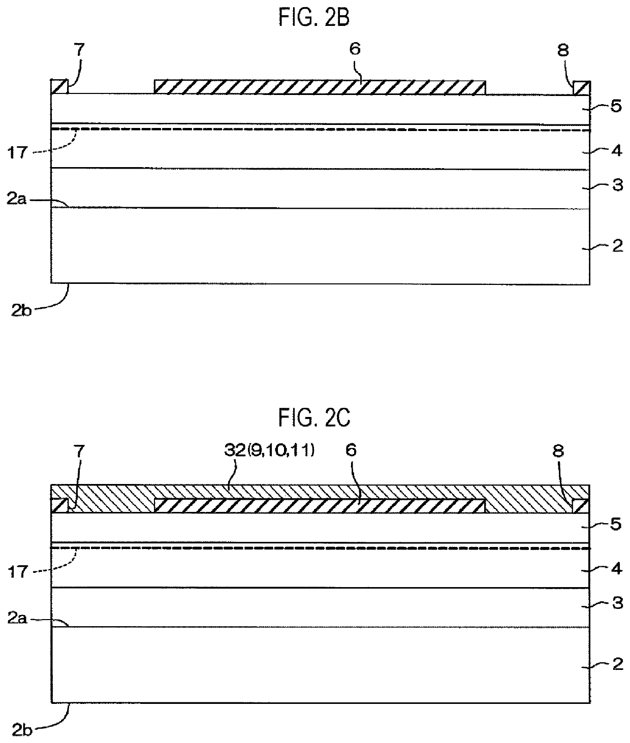
[0072]The nitride semiconductor device 1 includes a substrate 2, a buffer layer 3 formed over a front surface 2a of the substrate 2, a first nitride semiconductor layer 4 epitaxially grown on the buffer layer 3, and a second nitride semiconductor layer 5 epitaxially grown on the first nitride semiconductor layer 4.

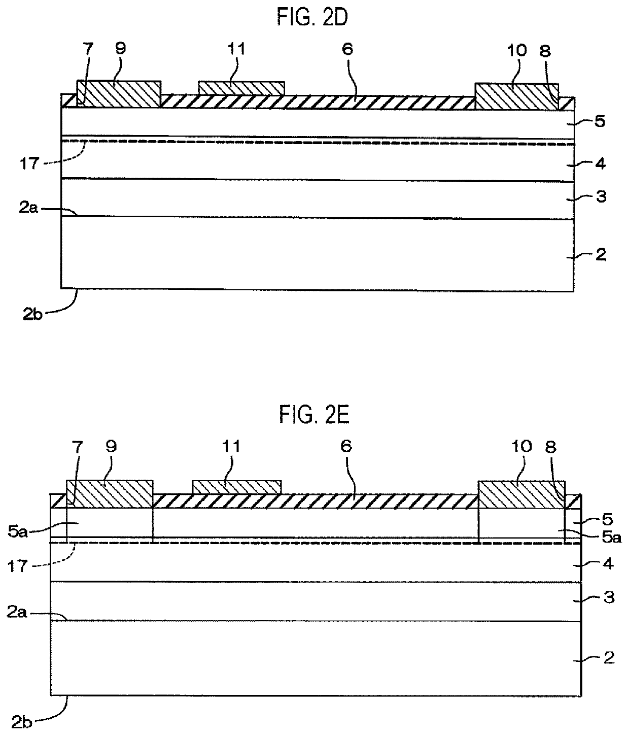
[0073]The nitride semiconductor device 1 further includes a gate-insulating film 6 formed over the second nitride semiconductor layer 5. The nitride semiconductor device 1 further includes a source electrode 9 and a drain electrode 10 (one of which may be a back-surface-drawing target electrode), which penetrate a source electrode contact hole 7 and a drain electrode contact hole 8 formed in the gate-insulating film 6 and make ohmic contact with the second nitride semiconductor layer 5. The source electrode 9 and the drain electrode 10 are s...

second embodiment

[0118]FIG. 7 is a sectional view for explaining a configuration of a nitride semiconductor device according to the present disclosure.

[0119]The nitride semiconductor device 1A includes a substrate 2, a buffer layer 3 formed over the front surface 2a of the substrate 2, a first nitride semiconductor layer 4 epitaxially grown on the buffer layer 3, and a second nitride semiconductor layer 5 epitaxially grown on the first nitride semiconductor layer 4.

[0120]The nitride semiconductor device 1A further includes a gate-insulating film 6 formed over the second nitride semiconductor layer 5. The nitride semiconductor device 1A further includes a source electrode 9 and a drain electrode 10 penetrating the source electrode contact hole 7 and the drain electrode contact hole 8 formed in the gate-insulating film 6 and making ohmic contact with the second nitride semiconductor layer 5. The source electrode 9 and the drain electrode 10 are spaced apart from each other.

[0121]The nitride semiconduc...

third embodiment

[0160]FIG. 11 is a schematic sectional view for explaining a configuration of a nitride semiconductor device according to the present disclosure.

[0161]The nitride semiconductor device 1B includes a substrate 2, a buffer layer 3 formed over the front surface 2a of the substrate 2, a first nitride semiconductor layer 4 epitaxially grown on the buffer layer 3, and a second nitride semiconductor layer 5 epitaxially grown on the first nitride semiconductor layer 4. The nitride semiconductor device 1B further includes a gate portion 70 formed over the second nitride semiconductor layer 5.

[0162]The nitride semiconductor device 1B further includes a passivation film 58 covering the second nitride semiconductor layer 5 and the gate portion 70, and a barrier metal film 59 laminated on the passivation film 58. The nitride semiconductor device 1B further includes a source electrode 62 and a drain electrode 63 penetrating the source electrode contact hole 60 and the drain electrode contact hole ...


PUM

PropertyMeasurementUnit
thicknessaaaaaaaaaa
thicknessaaaaaaaaaa
thicknessaaaaaaaaaa

Abstract

There is provided a nitride semiconductor device, including: a Si substrate including a front surface and a back surface; a buffer layer formed over the Si substrate; a first nitride semiconductor layer formed over the buffer layer; a second nitride semiconductor layer formed over the first nitride semiconductor layer; a gate electrode disposed over the second nitride semiconductor layer; a source electrode and a drain electrode electrically connected to the second nitride semiconductor layer, and disposed over the second nitride semiconductor layer to be spaced apart from the gate electrode that is interposed between the source electrode and the drain electrode; a back surface electrode pad formed over the back surface of the Si substrate; and a conductive path formed in the Si substrate, the buffer layer, the first nitride semiconductor layer, and the second nitride semiconductor layer.

Description

CROSS-REFERENCE TO RELATED APPLICATIONS[0001]This application is based upon and claims the benefit of priority from Japanese Patent Application No. 2018-054896, filed on Mar. 22, 2018, the entire contents of which are incorporated herein by reference.TECHNICAL FIELD[0002]The present disclosure relates to a nitride semiconductor device composed of a group III nitride semiconductor (hereinafter sometimes simply referred to as “nitride semiconductor”).BACKGROUND[0003]The group III nitride semiconductor refers to a semiconductor which utilizes nitrogen as a group V element in a group III-V semiconductor. Typical examples thereof are aluminum nitride (AlN), gallium nitride (GaN) and indium nitride (InN). In general, the group III nitride semiconductor may be expressed as AlxInyGa1-x-yN (0≤x≤1, 0≤y≤1, and 0≤x+y≤1).[0004]There is known a HEMT (High Electron Mobility Transistor) using a nitride semiconductor. The HEMT includes a Si substrate, an electron transit layer formed over the Si sub...

Claims


Application Information

Patent Timeline
Patent Type & Authority Patents(United States)
IPC IPC(8): H01L29/20H01L29/417H01L29/40H01L29/423H01L29/778H01L21/02H01L29/205
CPCH01L21/0262H01L29/41725H01L29/205H01L29/402H01L29/42356H01L21/0254H01L29/7787H01L29/2003H01L29/0847H01L29/66462H01L29/4175H01L29/1066
Inventor YOSHIMOCHI, KENICHI
Owner ROHM CO LTD
Why Eureka
Try Eureka