Refrigeration structure of semiconductor laser, and semiconductor laser and stack thereof

a semiconductor laser and refrigeration structure technology, applied in the field of lasers, can solve the problems of limited heat dissipation efficiency, semiconductor lasers tend to break down, and difficult use of conductive cooling type packaging structure in high-power devices, so as to reduce chip stress, avoid electrochemical corrosion, and be reliable

Active Publication Date: 2020-11-03
FOCUSLIGHT TECH
View PDF11 Cites 1 Cited by
  • Summary
  • Abstract
  • Description
  • Claims
  • Application Information

AI Technical Summary

Benefits of technology

[0008]In view of the above-described problems, it is one objective of the invention to provide a cooler of the semiconductor laser, a semiconductor laser comprising the cooler, and a stack of the semiconductor lasers, all of which can be applied to high power devices, and have high environmental adaptability and reliability.
[0015]1. The liquid cooler is employed, which satisfies the heat dissipation requirement of the high-power device, and the heat sink is electrically insulated; the connection surface of the electrode and the cooler is insulated by an insulating layer, thereby ensuring that the microchannels of the cooler are completely insulated during operation, avoiding electrochemical corrosion.
[0016]2. The laser chip does not directly contact the heat sink, which reduces the stress of the chip and saves the process of disposing the copper-tungsten release layer.
[0017]3. The positive and negative electrical connections under the premise of heat sink insulation are more reliable, especially the designed U-shaped connection piece has a simple structure, is convenient to use, and is very suitable for reliable use in semiconductor lasers. In the vertical stack structure, how to realize the electrical connection of the upper and lower coolers is a technical difficulty. In the present application, through the creative design of the U-shaped connection piece, the insulated cooler can be directly applied to the vertical stacked structure. Based on the U-shaped connection piece, the positive of each cooler is closely coupled with the negative of the cooler located thereon, and the insulating layer and the cooler are insulated through an insulation interlayer, which does not affect the characteristics of the electrical isolation of the cooler.

Problems solved by technology

Limited by the heat dissipation efficiency, the conductive cooling type packaging structure is difficult to use in high power devices.
1) Liquid-cooled semiconductor laser with microchannel: the heat dissipation of the heat sink with microchannel is good (because a plurality of tiny heat dissipation channels is disposed inside), higher power can be realized, but because the heat sink works in the charged state, the electrochemical corrosion tends to occur, which causes the problem of channel blockage after long-term use; in addition, the heat sink with microchannel poses high requirements for liquid water quality. Once the tap water is used or the water change is not timely, the semiconductor laser tends to break down.
2) Liquid-cooled semiconductor laser with macrochannel: the heat sink with macrochannel has a large liquid passage, which can effectively solve the problem of blockage of the heat sink; however, limited to the heat dissipation efficiency, the liquid-cooled semiconductor laser cannot be used in high power devices. The internal passage of the heat sink is large, which reduces the water quality requirements. However, because the heat sink works in the charged state, if the water quality is too bad (such as tap water), the semiconductor laser will break down due to the metal oxide obstructions caused by the electrochemical reaction during use.

Method used


Image

  • Refrigeration structure of semiconductor laser, and semiconductor laser and stack thereof
  • Refrigeration structure of semiconductor laser, and semiconductor laser and stack thereof
  • Refrigeration structure of semiconductor laser, and semiconductor laser and stack thereof

Examples


embodiment 1

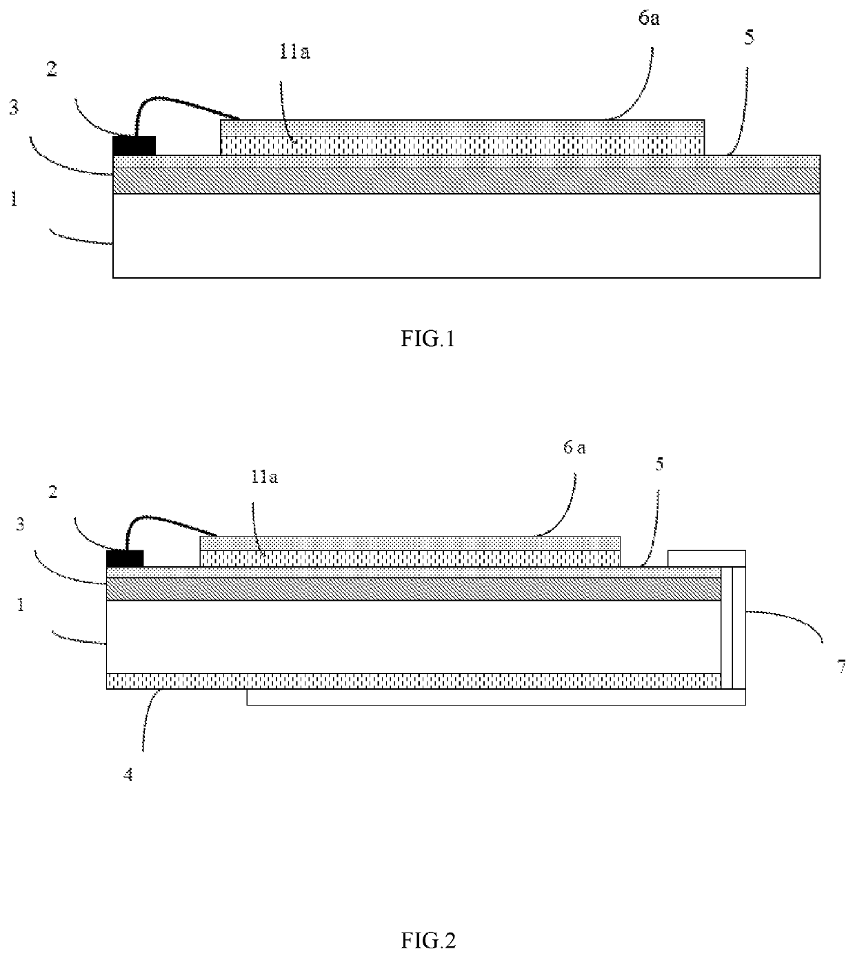
[0041]As shown in FIG. 1, a cooler of a semiconductor laser of the disclosure comprises a heat sink 1, a first insulation layer 3, a first electrical and thermal conductive layer 5, and a negative conductive layer 6a. The heat sink may be a liquid refrigerator having a liquid cooling circuit therein, and the negative conductive layer may be a negative copper piece. Of course, the heat sink and the negative conductive layer are not specifically defined in this embodiment. The cooler of the semiconductor laser can be equipped with a laser chip to manufacture a semiconductor laser.

[0042]Specifically, the heat sink comprises an upper surface and a lower surface. The first insulation layer is disposed on the upper surface to insulate the heat sink and the laser chip. The first electrical and thermal conductive layer 5 is disposed on the first insulation layer. The laser chip and the negative conductive layer are disposed on different positions of the first electrical and thermal conducti...

embodiment 2

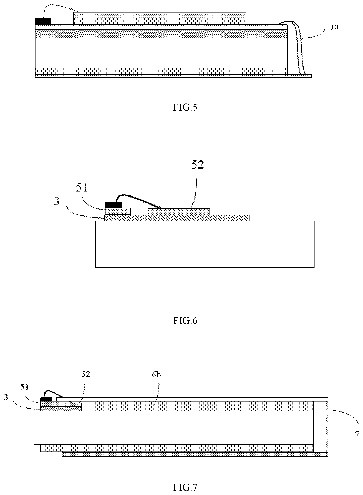
[0069]As shown in FIG. 6, a cooler of a semiconductor laser of the disclosure comprises a heat sink, a first insulation layer, and a first electrical and thermal conductive layer. The heat sink may be a liquid refrigerator having a liquid cooling circuit therein, and the negative conductive layer may be a negative copper piece.

[0070]The first insulation layer is disposed on the upper surface of the heat sink. The first electrical and thermal conductive layer is disposed on the first insulation layer. The first electrical and thermal conductive layer on the first insulation layer comprises two mutually insulated areas, that is, a positive area 51 and a negative area 52. The positive area is bonded to the positive surface of the laser chip, and the negative area is connected to the negative surface of the laser chip. Specifically, the positive area functions as a positive conductive layer, and the negative area functions as a negative conductive layer. When the laser chip is bonded on...

embodiment 3

[0095]FIG. 10 shows a cooler 100 of a semiconductor laser of the disclosure. As shown in FIG. 10, the cooler 100 of the disclosure comprises a heat sink 110, a positive conductive layer 120, a negative conductive layer 130 and a conductive conductor 140.

[0096]As shown in FIG. 10, the heat sink comprises an upper surface and a lower surface which are correspondingly disposed, and a side surface connecting the upper surface and the lower surface. It should be noted that the “upper” and “lower” of the upper and lower surfaces do not represent an absolute orientation. In this example, the upper surface is a first surface 111 and the lower surface is a second surface 112. The first surface 111 and the second surface 112 may be rectangular, having relatively long sides and relatively short sides, and the longer sides and the shorter sides are adjacent to each other. Optionally, the first surface and the second surface of the heat sink may also be other shapes, such as a square. If the fir...


PUM

PropertyMeasurementUnit
temperatureaaaaaaaaaa
conductiveaaaaaaaaaa
heat dissipation efficiencyaaaaaaaaaa

Abstract

Disclosed herein is a cooler of a semiconductor laser. The cooler includes a heat sink comprising a first surface and a second surface opposite the first surface; a first conductive layer and a second conductive layer, disposed on the first surface and not short-circuited to each other; and a conductive connector comprising a first end part, a second end part, and a first connection part connecting the first end part and the second end part. The first end part is on the first conductive layer. The second end part is on the second surface of the heat sink and insulated from the heat sink. The first connection part is disposed at a first non-opposite end of the first conductive layer on the heat sink.

Description

[0001]The present disclosure claims priority to Chinese Patent Application No. CN201610256531.6, filed with the Chinese Patent Office on Apr. 22, 2016, titled “LIQUID COOLED SEMICONDUCTOR LASER COMPRISING INSULATED HEAT SINK AND STACK THEREOF,” and to Chinese Patent Application No. CN201610256791.3, filed with the Chinese Patent Office on Apr. 22, 2016, titled “LIQUID COOLED SEMICONDUCTOR LASER COMPRISING INSULATING HEAT SINK.” The contents of all of the aforementioned applications, including any intervening amendments thereto, are incorporated herein by reference.FIELD OF THE INVENTION[0002]The disclosure belongs to the field of lasers, and more particularly to a cooler of the semiconductor laser, a semiconductor laser comprising the cooler, and a stack of the semiconductor lasers.BACKGROUND OF THE INVENTION[0003]Conventional packaging structures of the semiconductor lasers include two categories: liquid cooling type and conductive cooling type. Limited by the heat dissipation effi...

Claims


Application Information

Patent Timeline
Patent Type & Authority Patents(United States)
IPC IPC(8): H01S5/024H01S5/0233
CPCH01S5/02476H01S5/02423H01S5/02461H01S5/4025H01S5/4018H01S5/023H01S5/0233H01S5/0235H01S5/02345
Inventor LIU, XINGSHENGYU, DONGSHANLIANG, XUEJIEZHANG, LINBOJIA, YANGTAO
Owner FOCUSLIGHT TECH
Why Eureka
Try Eureka