Variable resistance random-access memory and method for write operation having error bit recovering function thereof

a random-access memory and variable resistance technology, applied in the field of semiconductor memory devices, can solve problems such as unstable state of variable resistance elements in variable resistance memory, and achieve the effect of suppressing the deterioration of the performance of the variable resistance random-access memory caused reducing the number of bits corrected by the error correction circui

Active Publication Date: 2021-02-02
WINBOND ELECTRONICS CORP
View PDF13 Cites 1 Cited by
  • Summary
  • Abstract
  • Description
  • Claims
  • Application Information

AI Technical Summary

Benefits of technology

[0011]In view of the above, the disclosure provides a variable resistance random-access memory which suppresses degradation of performance while recovering the memory cells that fail.
[0014]According to the disclosure, since the data of the memory cell determined as failure is rewritten when a predetermine event occurs, it is possible to recover the memory cell determined as failure. By recovering the memory cell determined as failure, the number of bits corrected by the error correction circuit can be reduced, and the deterioration of the performance of the variable resistance random-access memory caused by the error correction circuit can be suppressed.

Problems solved by technology

It is known that the state of the variable resistance element in the variable resistance memory becomes unstable as the SET / RESET write count (number of cycles) increases.

Method used


Image

  • Variable resistance random-access memory and method for write operation having error bit recovering function thereof
  • Variable resistance random-access memory and method for write operation having error bit recovering function thereof
  • Variable resistance random-access memory and method for write operation having error bit recovering function thereof

Examples


Embodiment Construction

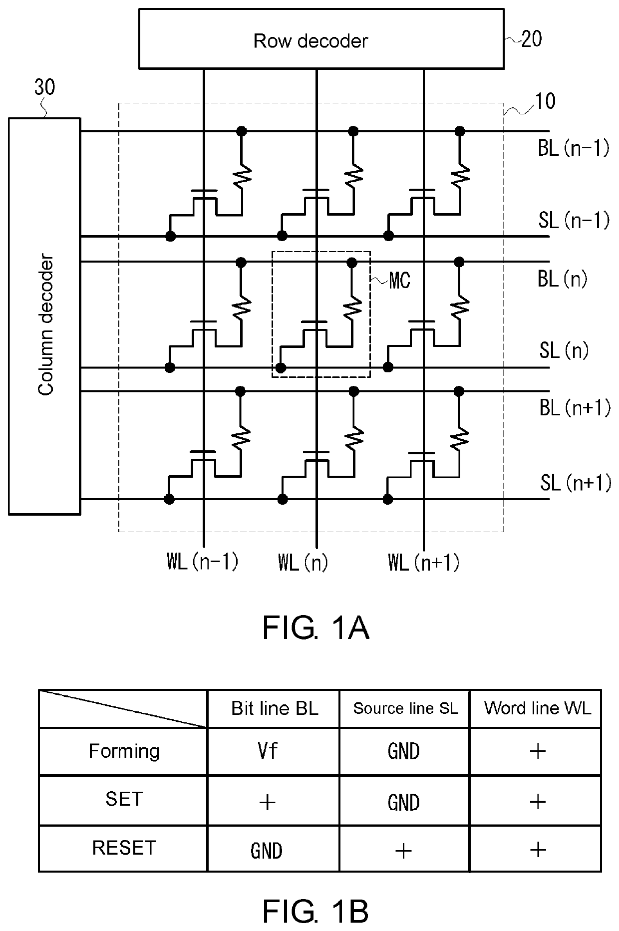
[0025]A variable resistance random-access memory (refers to RRAM) exemplified in the disclosure may be composed of one chip or may be embedded in one chip.

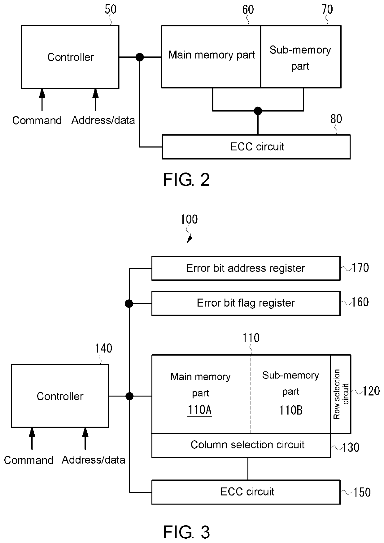
[0026]FIG. 3 is a block diagram showing a schematic configuration of a RRAM according to an embodiment of the disclosure. The RRAM 100 of this embodiment includes a memory array 110, a row selection circuit 120, a column selection circuit 130, a controller 140, an error checking and correcting (ECC) circuit 150, an error bit flag register 160, and an error bit address register 170. The memory array 110 has a plurality of memory cells arranged in rows and columns. The row selection circuit 120 selects a word line based on a row address. The column selection circuit 130 selects a bit line and a source line based on a column address and applies a corresponding bias voltage corresponding to an operation. The controller 140 controls each part of the RRAM 100 based on a command, an address, data, etc. received from the outside. The erro...


PUM


Abstract

Provided is a variable resistance random-access memory for suppressing degradation of performance by recovering a memory cell that fails. A variable resistance random-access memory of the disclosure includes a memory array, a row selection circuit, a column selection circuit, a controller, an error checking and correcting (ECC) circuit, an error bit flag register, and an error bit address register. The memory array includes a plurality of memory cells. The column selection circuit includes a sense amplifier and a write driver / read bias circuit. The error bit flag register stores bits for indicating presence / absence of an error bit in a write operation. The error bit address register stores an address of the error bit. The controller recovers the error bit when a predetermined event occurs.

Description

CROSS-REFERENCE TO RELATED APPLICATION[0001]This application claims the priority benefit of Japan application serial no. 2018-109926, filed on Jun. 8, 2019. The entirety of the above-mentioned patent application is hereby incorporated by reference herein and made a part of this specification.BACKGROUNDTechnical Field[0002]The disclosure relates to a semiconductor memory device, and more particularly to a variable resistance random-access memory using a variable resistance element.Description of Related Art[0003]A variable resistance memory stores data by applying a pulse voltage to a variable resistance element and setting the variable resistance element to a high resistance state or a low resistance state in a reversible and non-volatile manner. The variable resistance memory has the advantage that it can rewrite data at a low voltage, so the power consumption is low and the reading time is short (Patent Document 1: Japanese Laid-Open No. 2012-64286, Patent Document 2: Japanese Lai...

Claims


Application Information

Patent Timeline
Patent Type & Authority Patents(United States)
IPC IPC(8): G06F11/10G11C13/00
CPCG06F11/1012G11C13/004G11C13/0026G11C13/0028G11C13/0035G11C13/0069G11C13/0064G11C2013/0066G11C2213/79G11C2213/82G11C2013/0073G11C13/0033G11C2029/0411G11C29/52G06F11/1048G11C29/42
Inventor HATTORI, NORIO
Owner WINBOND ELECTRONICS CORP
Why Eureka
Try Eureka