Check patentability & draft patents in minutes with Patsnap Eureka AI!

Programmable resistance memory on thin film transistor technology

a technology of programmable resistance and transistor, which is applied in the direction of static storage, digital storage, instruments, etc., can solve the problems of large cell size of electrical fuse using silicided polysilicon, high cost of pcm embedded applications, and complex process steps for diodes

Active Publication Date: 2021-02-09
ATTOPSEMI TECH CO LTD
View PDF413 Cites 5 Cited by
  • Summary
  • Abstract
  • Description
  • Claims
  • Application Information

AI Technical Summary

Benefits of technology

The patent describes a programmable resistive memory that can be made using a non-single-crystal-silicon semiconductor film on an insulator substrate. The memory includes programmable resistive elements and selectors with active regions that can be programmed by applying voltages to different supply lines. The memory can be used in various electronic systems and can be programmed using a simple method. The technical effects of this invention include the ability to create a programmable resistive memory with a non-crystal-silicon semiconductor film on an insulator substrate, which can be used in various electronic systems, and can be programmed using a simple method.

Problems solved by technology

As a result, the cell size of an electrical fuse using silicided polysilicon tends to be very large.
Though this technology can reduce the PCM cell size to only 6.8 F2 (F stands for feature size), the diode requires very complicated process steps, such as Selective Epitaxial Growth (SEG), to fabricate, which would be very costly for embedded PCM applications.
The fuse elements 80, 84 in FIGS. 3(a) and 3(b) are relatively large structures which makes them unsuitable for some applications.

Method used


Image

  • Programmable resistance memory on thin film transistor technology
  • Programmable resistance memory on thin film transistor technology
  • Programmable resistance memory on thin film transistor technology

Examples


Embodiment Construction

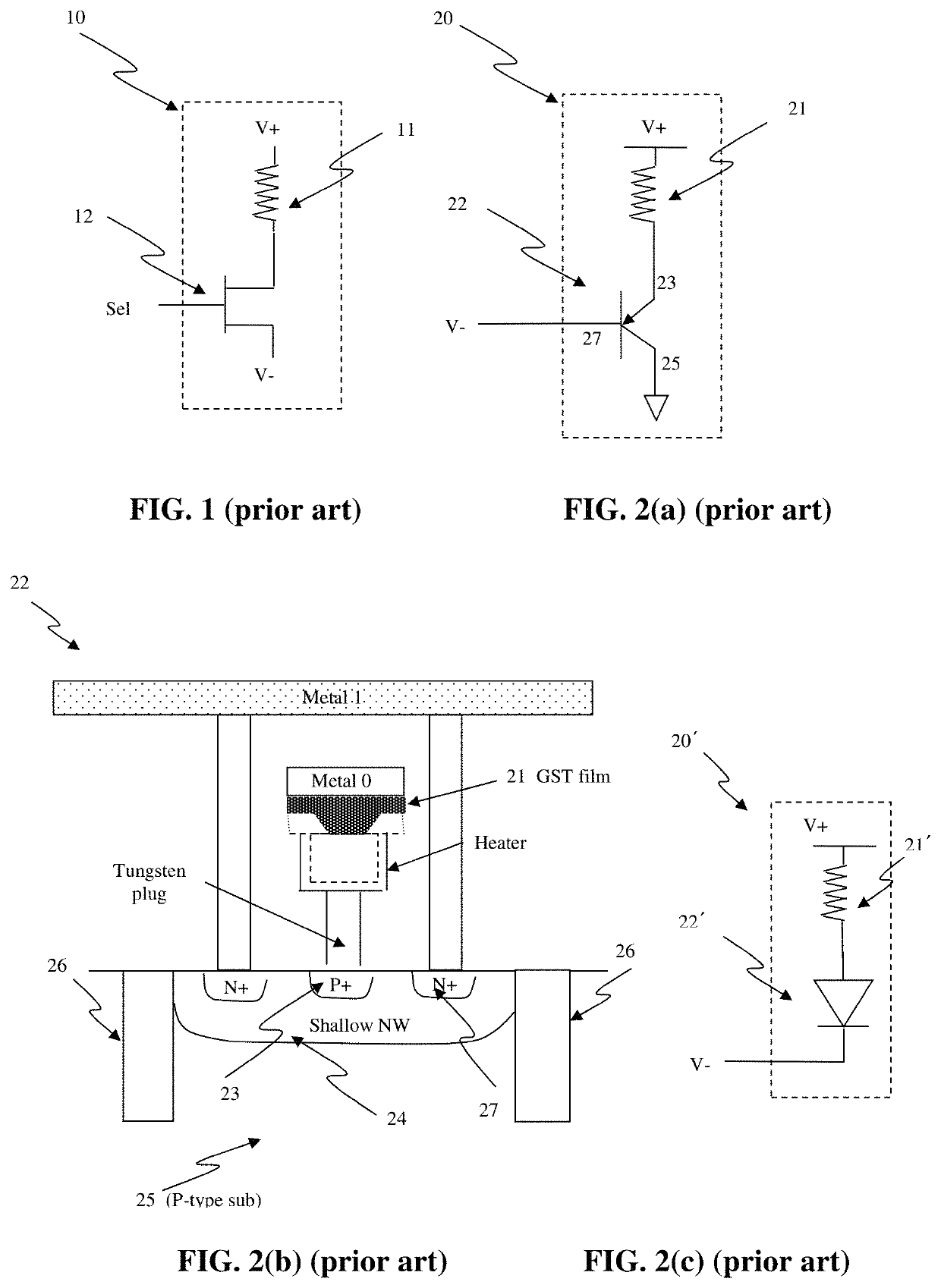
[0169]Embodiments disclosed herein use a P+ / N well junction diode as program selector for a programmable resistive device. The diode can comprise P+ and N+ active regions on an N well. Since the P+ and N+ active regions and N well are readily available in standard CMOS logic processes, these devices can be formed in an efficient and cost effective manner. For standard Silicon-On-Insulator (SOI), FinFET, or similar technologies, isolated active regions can be used to construct diodes as program selectors or as programmable resistive elements. The programmable resistive device can also be included within an electronic system.

[0170]Programmable resistive memory can be fabricated with a non-single-crystalline semiconductor formed on an insulator substrate. The non-single-crystalline semiconductor can be amorphous silicon, low-temperature polysilicon (LTPS), organic semiconductor, such as thiophene or PMMA, or metal oxide semiconductor, such as ITO or IGZO. The insulator substrate can be...


PUM


Abstract

Programmable resistive memory can be fabricated with a non-single-crystalline silicon formed on a flexible substrate. The non-single-crystalline silicon can be amorphous silicon, low-temperature polysilicon (LTPS), organic semiconductor, or metal oxide semiconductor. The flexible substrate can be glass, plastics, paper, metal, paper, or any kinds of flexible film. The programmable resistive memory can be PCRAM, RRAM, MRAM, or OTP. The OTP element can be a silicon, polysilicon, organic or metal oxide electrode. The selector in a programmable resistive memory can be a MOS or diode with top gate, bottom gate, inverted, staggered, or coplanar structures.

Description

CROSS-REFERENCE TO RELATED APPLICATIONS[0001]This application is a continuation-in-part of U.S. patent application Ser. No. 16 / 273,023, filed on Feb. 11, 2019 and entitled “FULLY TESTIBLE OTP MEMORY, which is hereby incorporated herein by reference, which is a continuation-in-part of U.S. patent application Ser. No. 15 / 708,116, filed on Sep. 18, 2017 and entitled “OTP MEMORY WITH HIGH DATA SECURITY, which is hereby incorporated herein by reference, which is also a continuation-in-part of U.S. patent application Ser. No. 15 / 422,266, filed on Feb. 1, 2017 and entitled “Method and Structure for Reliable Electrical Fuse Programming,” which is hereby incorporated herein by reference, which is a continuation of U.S. patent application Ser. No. 14 / 485,696, filed on Sep. 13, 2014 and entitled “Method and Structure for Reliable Electrical Fuse Programming,” which is a continuation-in-part of U.S. patent application Ser. No. 13 / 835,308, filed on Mar. 15, 2013 and entitled “Circuit and System ...

Claims


Application Information

Patent Timeline
Patent Type & Authority Patents(United States)
IPC IPC(8): G11C17/16G11C29/02G11C17/18
CPCG11C17/16G11C17/18G11C29/027G11C13/0002G11C13/003G11C17/165G11C2029/5006G11C2213/33G11C2213/80
Inventor CHUNG, SHINE C.
Owner ATTOPSEMI TECH CO LTD
Features
  • R&D
  • Intellectual Property
  • Life Sciences
  • Materials
  • Tech Scout
  • Unparalleled Data Quality
  • Higher Quality Content
  • 60% Fewer Hallucinations
Learn More