Tunable bandpass filter

a bandpass filter and bandpass technology, applied in the field of tunable bandpass filters, can solve the problems of difficult to reduce filter losses in the high-frequency band, add to losses, and extremely difficult filters, and achieve the effects of reducing the number of components, reducing the generation of losses, and simple structur

Active Publication Date: 2021-03-09
NEC CORP
View PDF9 Cites 0 Cited by
  • Summary
  • Abstract
  • Description
  • Claims
  • Application Information

AI Technical Summary

Benefits of technology

[0010]The tunable bandpass filter according to the present invention is capable of adjusting the position of the dielectric plate with respect to the resonance rod by driving, through use of an actuator or the like, the driving unit attached to the dielectric plate. The driving unit is capable of adjusting the position of the dielectric plate in two directions, that is, in directions parallel and perpendicular to the principal surface thereof. The driving unit is capable of changing the bandwidth through position adjustment in parallel direction and the center frequency through position adjustment in perpendicular direction. Thus, the tunable bandpass filter according to the present invention is capable of controlling only the bandwidth while keeping the center frequency constant.
[0011]The tunable bandpass filter according to the present invention is designed to control the bandwidth through position adjustment of the dielectric plate alone. Accordingly, even when a plurality of filters of different bandwidths are integrated into a single filter, it is unnecessary to adjust individual filters by using coupling adjusting screws as opposed to the related art, which offers a simple structure with reduced number of components.
[0012]The tunable bandpass filter according to the present invention is designed in such a way as not to use a variable capacitance element such as a varactor diode in the control of the bandwidth, which reduces generation of losses.

Problems solved by technology

However, the filter according to the related art uses a PCB and it is difficult to reduce filter losses in a high-frequency band.
Moreover, the filter according to the related art uses a variable capacitance element like a varactor diode, which adds to the losses.
Thus, it is extremely difficult for the filter according to the related art to reduce the losses.
A multi-stage filter includes a large number of components, which leads to a complicated structure and a high cost.
However, PTL 1 or PTL2 does not disclose a technique to control both of the center frequency and the bandwidth.

Method used


Image

  • Tunable bandpass filter
  • Tunable bandpass filter
  • Tunable bandpass filter

Examples


first example embodiment

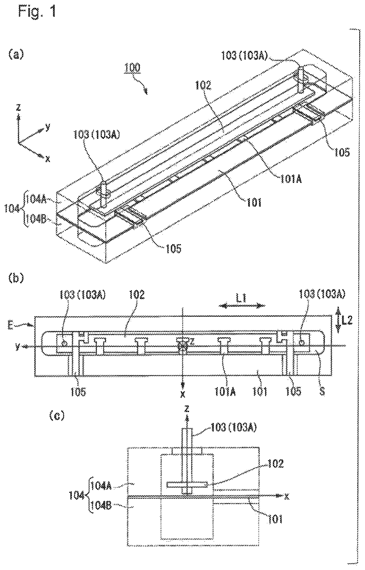
[0021]A configuration of a tunable bandpass filter according to a first example embodiment of the present invention will be described. FIG. 1 view (a) is a perspective view of a tunable bandpass filter 100 according to the example embodiment. The tunable bandpass filter 100 includes: a conductive member 101 including a plurality of resonance rods 101A; a dielectric plate 102; a driving unit 103 for driving the dielectric plate 102; and a waveguide 104 containing at least the resonance rods 101A and the dielectric plate 102.

[0022]The shape of the conductive member 101 is not limited but is preferably a flat plate-shaped member. In the following example, it is assumed that the conductive member 101 is a metallic plate. The plurality of resonance rods 101A are aligned in a single plane and protrude from the conductive member 101. The principal surface of the conductive member 101 as a metallic plate is preferably approximately parallel to the single plane in which the resonance rods 10...

second example embodiment

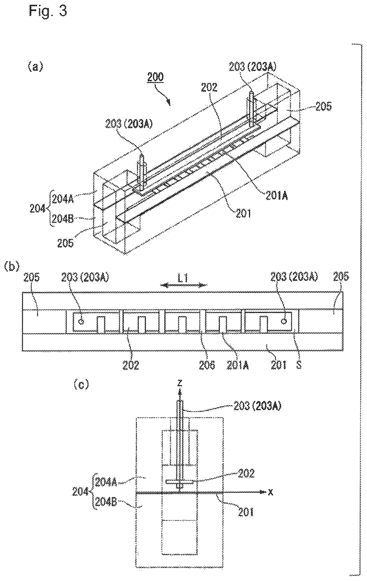
[0042]A configuration of a tunable bandpass filter 200 according to a second example embodiment of the present invention will be described.

[0043]FIG. 3 view (a) is a perspective view of the tunable bandpass filter 200 according to the example embodiment.

[0044]FIG. 3 view (b) is a bottom view of the tunable bandpass filter 200 of FIG. 3 view (a) as viewed from the side where a dielectric plate 202 is not disposed (bottom side of FIG. 3 view (a)). In FIG. 3 view (b), a waveguide 204 as an external conductor is illustrated see-through in order to clarify the structure of a conductive member 201.

[0045]FIG. 3 view (c) is a side view of the tunable bandpass filter 200 of FIG. 3 view (a) as viewed from one end of the waveguide 204 in the longitudinal direction L1. In order to clarify the structure of the dielectric plate 202 and a driving unit 203, the waveguide 204 is also illustrated see-through in FIG. 3 view (c).

[0046]Note that, in FIG. 3, a reference sign 201A indicates a resonance ro...

third example embodiment

[0048]A configuration of a tunable bandpass filter 300 according to a third example embodiment of the present invention will be described.

[0049]FIG. 4 view (a) is a perspective view of the tunable bandpass filter 300 according to the example embodiment.

[0050]FIG. 4 view (b) is a bottom view of the tunable bandpass filter 300 of FIG. 4 view (a) as viewed from the side where a dielectric plate 302 is not disposed (bottom side of FIG. 4 view (a)). In FIG. 4 view (b), a waveguide 304 as an external conductor is illustrated see-through in order to clarify the structure of a conductive member 301.

[0051]FIG. 4 view (c) is a side view of the tunable bandpass filter 300 of FIG. 4 view (a) as viewed from one end of the waveguide 304 in the longitudinal direction L1. In order to clarify the structure of the dielectric plate 302 and a driving unit 303, the waveguide 304 is also illustrated see-through in FIG. 4 view (c).

[0052]Note that, in FIG. 4, a reference sign 303A indicates a rod-shaped me...


PUM

PropertyMeasurementUnit
conductiveaaaaaaaaaa
passband widthaaaaaaaaaa
frequencyaaaaaaaaaa

Abstract

This tunable bandpass filter is provided with: a conductive member having a plurality of resonance rods protruding so as to be aligned in a single plane; a dielectric plate disposed parallel to the single plane; a drive part which is attached to the dielectric plate and drives the dielectric plate in directions parallel and perpendicular to the single plane; and a waveguide containing at least the resonance rods and the dielectric plate.

Description

CROSS REFERENCE TO RELATED APPLICATIONS[0001]This application is a National Stage of International Application No. PCT / JP2017 / 011712 filed Mar. 23, 2017, claiming priority based on Japanese Patent Application No. 2016-072641 filed Mar. 31, 2016, the entire disclosure of which is incorporated herein.TECHNICAL FIELD[0002]The present invention relates to a tunable bandpass filter capable of controlling a microwave or millimeter-wave passband width.BACKGROUND ART[0003]Filters needed in microwave or millimeter-wave band applications typically require low losses. In particular, the requirement is high in devices for acquiring high output. For the purpose of integrating devices having separate bandwidths into a single device, these filters require a variable bandwidth and low losses.[0004]A related art discloses a filter disposed on a Printed Circuit Board (PCB) that is capable of controlling the bandwidth through introduction of an additional variable capacitance by using a varactor diode...

Claims


Application Information

Patent Timeline
Patent Type & Authority Patents(United States)
IPC IPC(8): H01P1/205H01P1/208H01P7/04H01P7/10
CPCH01P1/205H01P1/2084H01P7/04H01P7/10
Inventor IWANAKA, DAISUKE
Owner NEC CORP
Why Eureka
Try Eureka