Optoelectronic device and method of manufacturing the same

a technology of optoelectronic devices and manufacturing methods, applied in the direction of optical elements, optical waveguide light guides, instruments, etc., can solve the problems of large device size, low variation tolerance of resonator-type electro-optic modulators, poor si material, etc., to reduce manufacturing costs, reduce optical loss, and simplify the process

Active Publication Date: 2021-04-13
KOOKMIN UNIV IND ACAD COOP FOUND
View PDF10 Cites 0 Cited by
  • Summary
  • Abstract
  • Description
  • Claims
  • Application Information

AI Technical Summary

Benefits of technology

[0008]The inventive concept is directed to an optoelectronic device that minimizes optical loss and reduces a manufacturing cost with a simplified process and a method of manufacturing the optoelectronic device.

Problems solved by technology

However, due to an indirect band gap characteristic of Si, Si material is usually poor and inappropriate for forming an electro-absorption modulator.
Instead, Si-based Mach-Zehnder type and resonator-type electro-optic modulators are being used, but the Mach-Zehnder type modulator has a problem of large device size due to silicon's small electro-optic coefficient and the resonator-type electro-optic modulator has a problem of low variation-tolerance.
The GeSi-based optoelectronic device needs to have a relatively short active region because some residual absorption due to the indirect band gap characteristic inevitably causes optical loss.
However, the SOI substrate is about 10 times more expensive than the bulk silicon substrate, resulting in an increase in the manufacturing cost.
Furthermore, because the common electronic integrated circuit (IC) chip is normally fabricated on bulk Si substrate, the optoelectronic devices designed on the SOI substrate cannot be fabricated and integrated together with electronic integrated-circuit (IC) chip.

Method used


Image

  • Optoelectronic device and method of manufacturing the same
  • Optoelectronic device and method of manufacturing the same
  • Optoelectronic device and method of manufacturing the same

Examples


Embodiment Construction

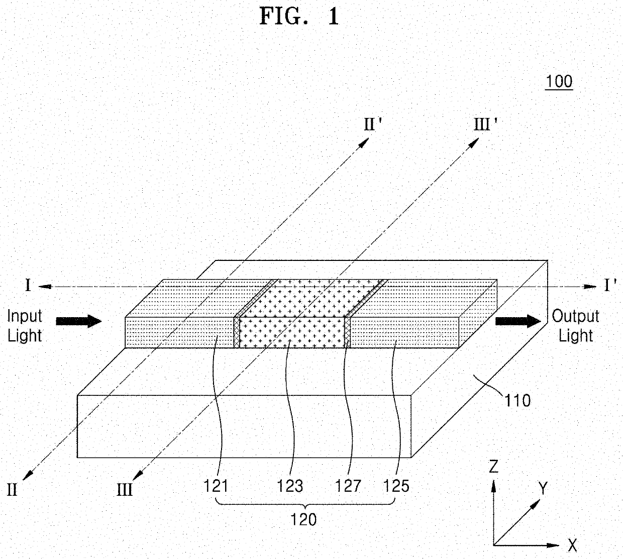
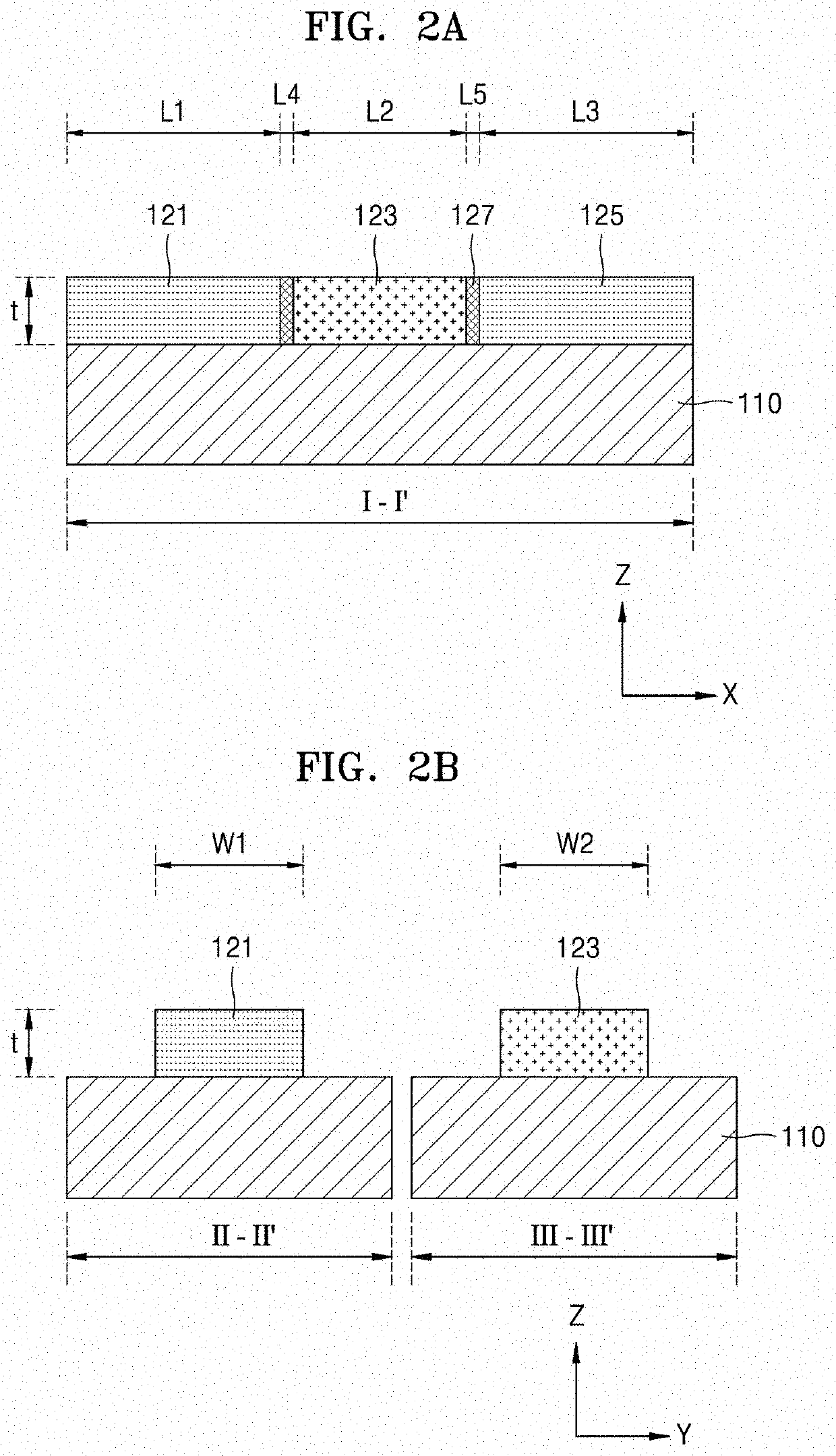
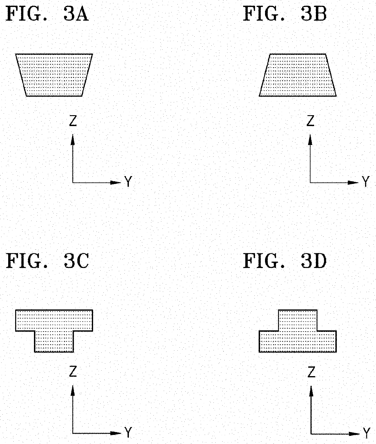
[0034]Reference will now be made in detail to embodiments, examples of which are illustrated in the accompanying drawings, wherein like reference numerals refer to like elements throughout. In this regard, the present embodiments may have different forms and should not be construed as being limited to the descriptions set forth herein. Accordingly, the embodiments are merely described below, by referring to the figures, to explain aspects of the present description.

[0035]It will be understood that, although the terms first, second, etc. may be used herein to describe various members, components, regions, layers, and / or sections, these members, components, regions, layers, and / or sections should not be limited by these terms. These terms do not denote any order, quantity, or importance, but rather are only used to distinguish one component, region, layer, and / or section from another component, region, layer, and / or section. Thus, a first member, component, region, layer, or section d...


PUM

PropertyMeasurementUnit
lengthaaaaaaaaaa
lengths L1aaaaaaaaaa
band gap wavelengthaaaaaaaaaa

Abstract

There is provided an optoelectronic device including: first and second optical waveguides arranged on a bulk silicon substrate to be spaced apart from each other in a first direction parallel to an upper surface of the bulk silicon substrate; and an active region interposed between the first and second optical waveguides on the bulk silicon substrate such that one side of the active region contacts the first optical waveguide and the other side contacts the second optical waveguide portion, wherein the first and second optical waveguides and the active region include germanium-silicon (GeSi) alloy.

Description

CROSS-REFERENCE TO RELATED APPLICATIONS[0001]This application claims the benefit of Korean Patent Application No. 10-2018-0165097, filed on Dec. 19, 2018, in the Korean Intellectual Property Office, the disclosure of which is incorporated herein in its entirety by reference.BACKGROUND1. Field[0002]The inventive concept relates to an optoelectronic device and a method of manufacturing the same, and more particularly, to an optoelectronic device integrated with a passive optical device and an active optical device based on germanium-silicon (GeSi) / Si and a method of manufacturing the same.2. Description of the Related Art[0003]In general, a silicon (Si) based modulator has been widely used as an optoelectronic device. However, due to an indirect band gap characteristic of Si, Si material is usually poor and inappropriate for forming an electro-absorption modulator. Instead, Si-based Mach-Zehnder type and resonator-type electro-optic modulators are being used, but the Mach-Zehnder type...

Claims


Application Information

Patent Timeline
Patent Type & Authority Patents(United States)
IPC IPC(8): G02B6/12G02B6/13
CPCG02B6/12004G02B6/13G02B2006/12061G02B2006/12142G02B6/136Y02E10/52H01L31/02327H01L31/032H01L31/125H01L31/18H01L31/054
Inventor AHN, DONGHWAN
Owner KOOKMIN UNIV IND ACAD COOP FOUND
Why Eureka
Try Eureka