Multi-mode waveguide using space-division multiplexing

Inactive Publication Date: 2017-12-14
RGT UNIV OF CALIFORNIA
View PDF6 Cites 1 Cited by
  • Summary
  • Abstract
  • Description
  • Claims
  • Application Information

AI Technical Summary

Benefits of technology

[0017]The inventive approach increases the data transfer capacity of a waveguide using the degree of freedom provided by multiple guided spatial modes by associating one carrier signal with each spatial mode. It is distinct from, but compatible with, other multiplexing techniques that operate using a different degree of freedom, e.g., wavelength-division multiplexing (WDM) that uses spectral modes supported by the waveguide.
[0018]The inventive SDM coupling approach advantageously minimizes optical loss by limiting the perturbations to the space where the modes maximally overlap. For integrated waveguides the dominant source of loss is scattering produced by roughness in the waveguide sidewalls. Consequently, increasing the waveguide dimensions will actually reduce loss because less of the mode overlaps with the waveguide sidewalls. This can be contrasted with prior art single mode couplers, which devices have perturbations on the outside of waveguides where the mode overlap is negligible. As a result, the contribution of such perturbations to the coupling coefficient is negligible while the loss contributions from increased sidewall area is nontrivial.
[0019]In an aspect of the invention, a

Problems solved by technology

The conventional solution for this problem, wavelength-division multiplexing (WDM) in single-mode fiber links, suffers from a number of complex scaling challenges ranging from the cost of discrete WDM components to thermal management issues.
However, it should be noted that such an integrated system would be costly and complex due to the need to integrate and control the laser sources, remove heat, and stabilize the system for operation in practical environments (e.g., temperature stabilization, monitoring the lasers and receivers on WDM grid, etc.).
In multimode fiber (MMF) this approach has proven to be unfea

Method used


Image

  • Multi-mode waveguide using space-division multiplexing
  • Multi-mode waveguide using space-division multiplexing
  • Multi-mode waveguide using space-division multiplexing

Examples


Example

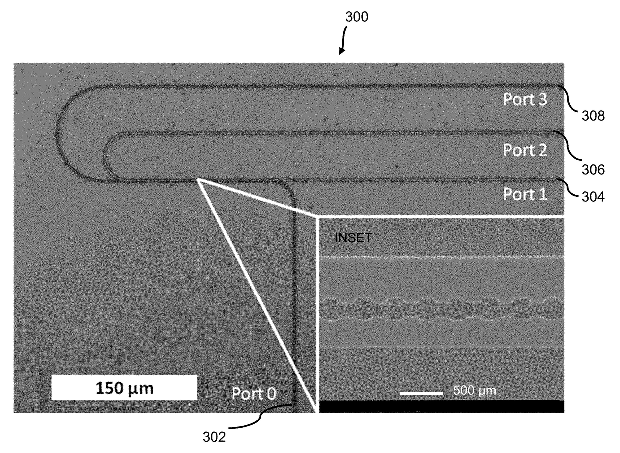
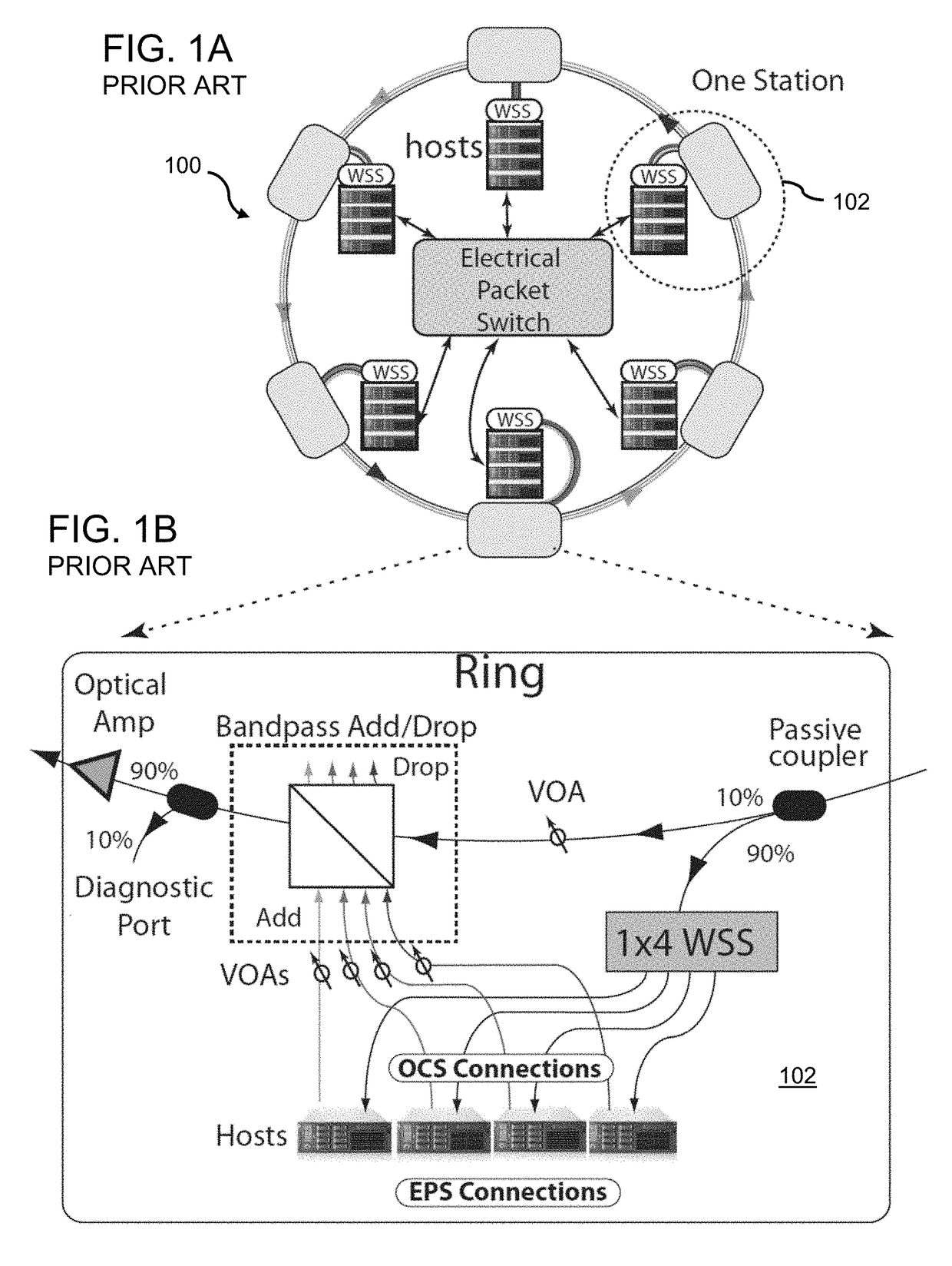
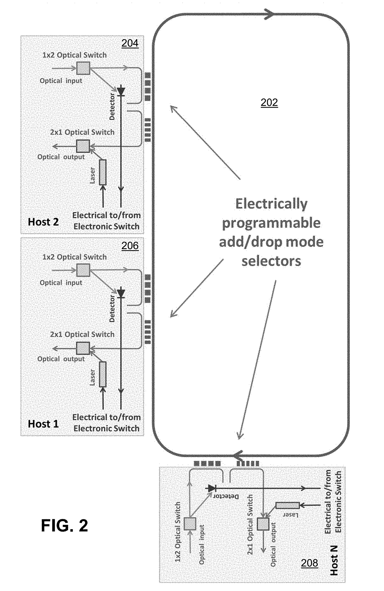
[0031]FIG. 2 illustrates provides an example of a hybrid SDM photon chip architecture incorporating the inventive technology. The architecture follows the structure of a MORDIA datacenter such as described by Farrington, et al. in “A 10 μs Hybrid Optical-circuit / Electrical-Packet Network for Datacenters,”Proc. IEEE / OSA Fiber Commun. Conf., March 2013, Paper OW3H.3, and Farrington, et al., “Hunting Mice with Microsecond Circuit Switches,” in ACM HotNets, Redmond, Wash., 2012, each of which is incorporated herein by reference. The switch includes an electronic packet switch 202 with j hosts, “Host 1”204, “Host 2”206, and “Host N”208. In embodiments of the invention, a number of carrier signals are multiplexed into a waveguide by using the different guided modes of the waveguide. The coupling between arbitrary modes is accomplished by periodically structuring the waveguides. The effect of periodically structuring the waveguide may be described using the paradigm of the electromagnetic ...


PUM


Abstract

A multi-mode optical waveguide device is formed from a plurality of periodically structured waveguides, where each waveguide is configured to guide a carrier signal comprising one spatial mode of a plurality of spatial modes and has at least one segment of each waveguide with a waveguide width that periodically changes along a waveguide path to induce coupling between pairs of spatial modes. In some embodiments, the at least one segment is disposed at a location along the waveguide path at which maximal mode overlap occurs. The waveguide device may be used as for space-division multiplexing and as an optical switch.

Description

RELATED APPLICATIONS[0001]This application claims the benefit of the priority of U.S. Provisional Application No. 62 / 104,550, filed Jan. 16, 2015, which is incorporated herein by reference in its entirety.GOVERNMENT RIGHTS[0002]The present invention was made with government support under Grant No. Y502629 (EEC-0812072) awarded by the National Science Foundation. The government has certain rights in the invention.FIELD OF THE INVENTION[0003]The present invention relates to a system and method for multiplexing multiple carrier signals into a waveguide by using different guided spatial modes supported by the waveguide.BACKGROUND[0004]The widespread adoption of cloud computing has led to the construction of data center networks that support up to hundreds of thousands of servers, requiring internal communications at high server-to-server, or bi-section, bandwidths that are orders of magnitude greater than their connections to end users. These networks must scale with the rapid growth in...

Claims


Application Information

Patent Timeline
IPC IPC(8): G02B6/14G02B6/125H04J14/04G02F1/313G02B6/122G02B6/12
CPCG02B6/14G02B6/1228G02F1/313G02B2006/12038G02B6/125G02B2006/12061H04J14/04G02B6/136
Inventor GRIECO, ANDREWFAINMAN, YESHAIAHUPORTER, GEORGE
Owner RGT UNIV OF CALIFORNIA
Why Eureka
Try Eureka