Multi-Junction VCSEL with Compact Active Region Stack

a technology of active region stack and vcsel, which is applied in the direction of semiconductor lasers, laser details, electrical apparatus, etc., can solve the problems of inability to control and match as much as possible the two oxide apertures, inherent problems with respect to current spreading and modal instability, and inherently limited optical output power that may be delivered by an individual vcsel device, etc., to achieve the effect of minimizing optical loss and increasing optical confinemen

Active Publication Date: 2022-06-16
II VI DELAWARE INC
View PDF7 Cites 0 Cited by
  • Summary
  • Abstract
  • Description
  • Claims
  • Application Information

AI Technical Summary

Benefits of technology

[0008]The problems remaining in these prior art approaches is addressed by the present invention, which relates to a high output power VCSEL having two or more active regions formed in a stack and separated by a tunnel junction, the stack itself compacted in terms of the number of individual layers so as to confine lateral current spread, increasing optical confinement and minimizing optical loss.
[0009]A multi-junction VCSEL is formed as a compact structure that reduces lateral current spreading by reducing the spacing between adjacent active regions in the stack of such regions used to form the multi-junction device. In particular, at least two of the active regions within the stack are located at adjacent peaks of the intensity profile of the VCSEL, with an intervening tunnel junction positioned at a trough between the two peaks. The alignment of the active regions with the peaks maximizes the generated optical power, while the alignment of the tunnel junction with the trough minimizes optical loss. The close spacing on adjacent peaks forms a compact structure (which may even include a cavity having a sub-λ optical length) that lessens the total path traveled by carriers and therefore reduces lateral current spread.

Problems solved by technology

The optical output power that may be delivered by an individual VCSEL device has been found to be inherently limited by its relatively small-sized aperture, a requirement to prevent lateral spreading of the injected current as it traverses through the depth of the device structure.
While an increase in output power may be obtained by the use of multiple active regions, the inherent problems with respect to current spreading and modal instability remain.
This has the disadvantage of having to control and match as much as possible the two oxide aperture sizes, which depends on a variety of fabrication process variables including, but not limited to, the mesa etch profile of the VCSEL, aluminum composition and thickness of the layers designated for creation of the oxide apertures, etc.
Besides the fabrication difficulties, the inclusion of a second oxide aperture results in a higher electrical resistance within the device (thus resulting in higher voltage requirements, lower wall plug efficiency, and higher self-heating; these factors all contributing to lower optical output power).

Method used


Image

  • Multi-Junction VCSEL with Compact Active Region Stack
  • Multi-Junction VCSEL with Compact Active Region Stack
  • Multi-Junction VCSEL with Compact Active Region Stack

Examples


Embodiment Construction

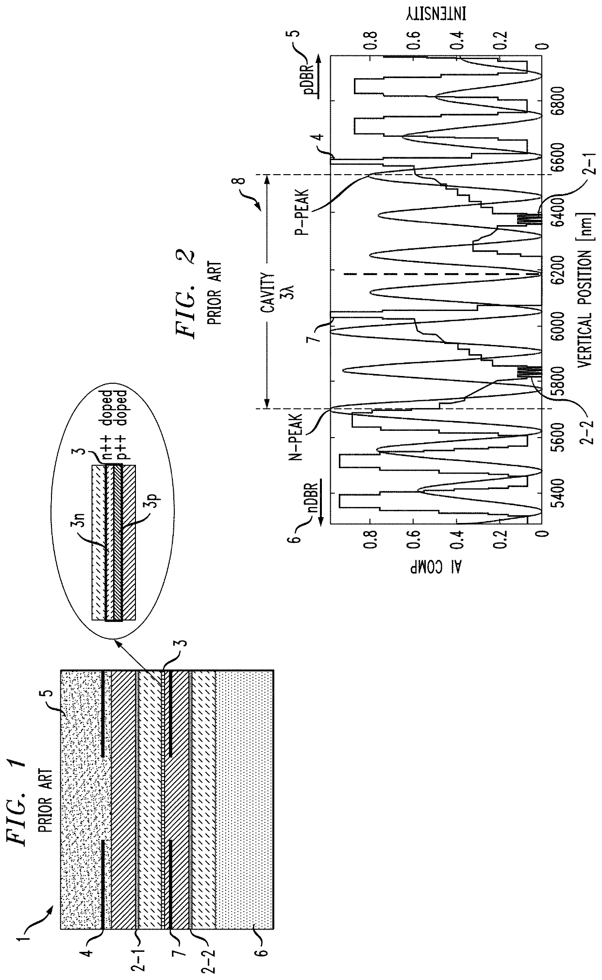
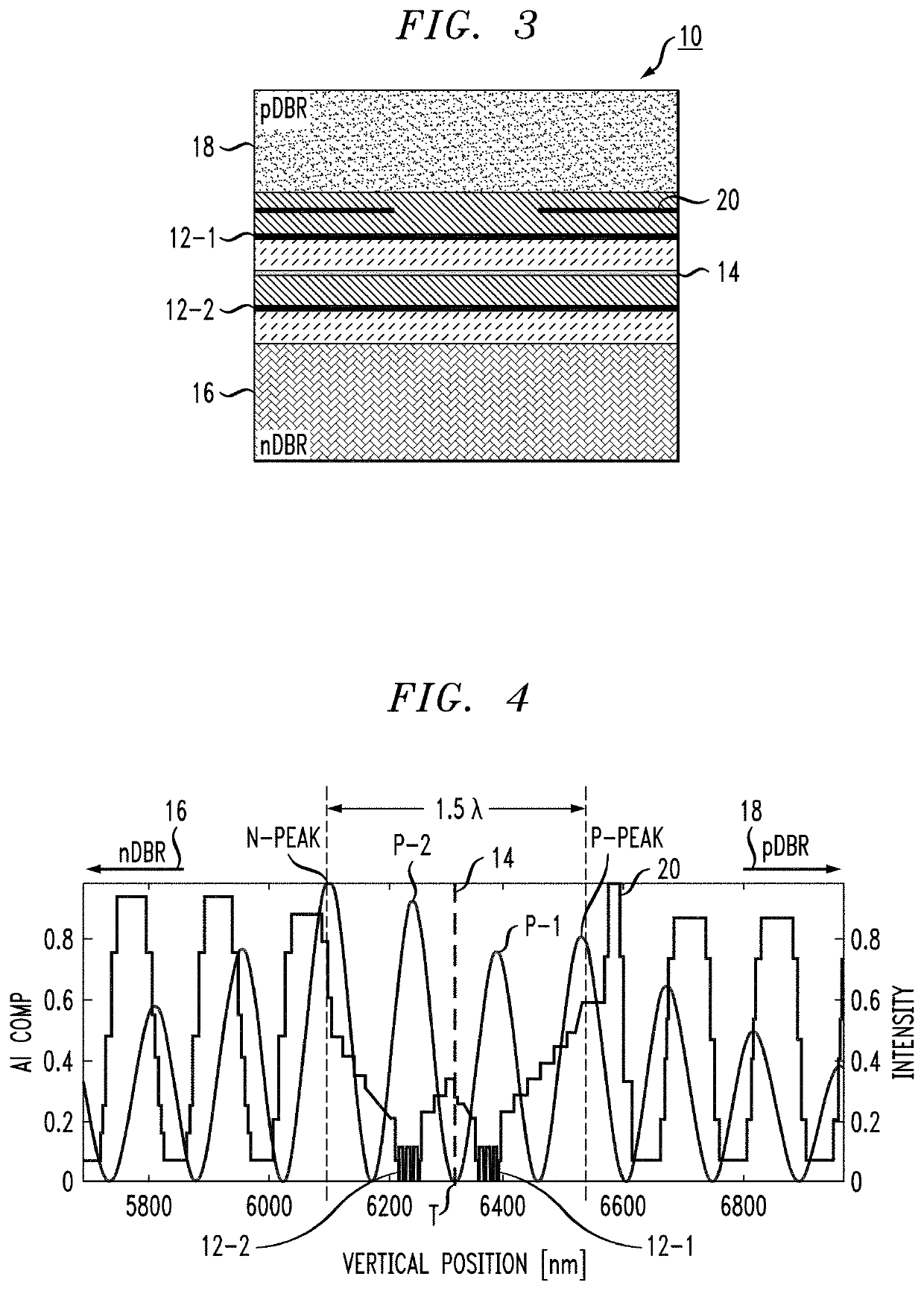
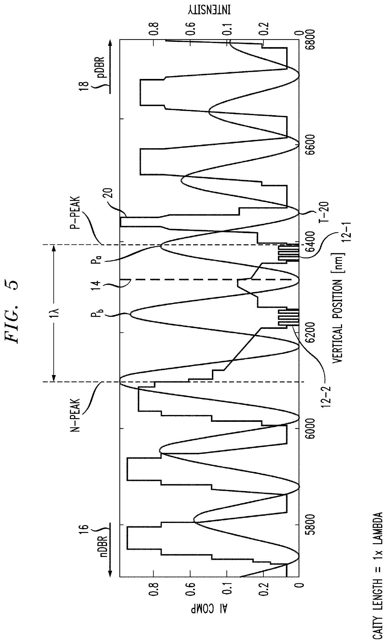
[0027]FIG. 1 is a simplified view of a conventional prior art VCSEL 1, formed to include a pair of “stacked” active regions 2-1 and 2-2. A tunnel junction 3 is positioned between active regions 2-1 and 2-2 as shown, and is used to move holes and electrons between the active regions in a manner that energizes both regions from the bias current applied as an input to the structure (not shown). Tunnel junction 3, as shown in the enlarged portion of FIG. 1, comprises a highly-doped n-type layer 3n formed over a highly-doped p-type layer 3p. The doping levels need to on the order of 1×1019 cm−3 or greater in order to allow tunneling of carriers through the tunnel junction. A conventional oxide aperture layer 4 is shown a formed within a p-type distributed Bragg reflector (pDBR) 5, where the created optical output is typically emitted from pDBR 5. An n-type DBR, shown as nDBR 6 forms the bottom reflective portion of the laser structure.

[0028]Under reverse bias, tunnel junction 3 is used t...


PUM

PropertyMeasurementUnit
refractive indexaaaaaaaaaa
conductivity typeaaaaaaaaaa
conductivityaaaaaaaaaa

Abstract

A multi-junction VCSEL is formed by as a compact structure that reduces lateral current spreading by reducing the spacing between adjacent active regions in the stack of such regions used to from the multi-junction device. At least two of the active regions within the stack are located adjacent peaks of the intensity profile of the VCSEL, with an intervening tunnel junction positioned at a trough between the two peaks. The alignment of the active regions with the peaks maximizes the generated optical power, while the alignment of the tunnel junction with the trough minimizes optical loss. The close spacing on adjacent peaks forms a compact structure (which may even include a cavity having a sub-λ optical length) that lessens the total path traveled by carriers and therefore reduces lateral current spread.

Description

CROSS-REFERENCE TO RELATED APPLICATIONS[0001]This application is a continuation of U.S. patent application Ser. No. 16 / 951,020, filed Nov. 18, 2020 and incorporated herein in its entirety.TECHNICAL FIELD[0002]The present invention relates to a vertical cavity surface emitting laser (VCSEL) device and, more particularly, to a VCSEL having two or more active regions formed in a stack and separated by a tunnel junction, the stack itself compacted in terms of the number of individual layers so as to confine lateral current spread, increasing optical confinement and minimizing optical loss.BACKGROUND OF THE INVENTION[0003]A VCSEL has a laser cavity that is sandwiched between and defined by two mirror stacks. A VCSEL is typically fabricated on a semiconductor substrate (in many cases a GaAs or InP substrate), with a “bottom” mirror stack formed on the top surface of the substrate, and then covered by the laser cavity and “top” mirror stack. Each mirror stack includes a number of epitaxial...

Claims


Application Information

Patent Timeline
Patent Type & Authority Applications(United States)
IPC IPC(8): H01S5/30H01S5/183
CPCH01S5/3095H01S5/3416H01S5/18311H01S5/18397H01S5/18308H01S5/18322H01S5/18361H01S5/18313H01S5/18383H01S5/18358H01S5/1833
Inventor TANDOI, GIUSEPPE
Owner II VI DELAWARE INC
Why Eureka
Try Eureka