Multi-piece fiber optic component and manufacturing technique

a fiber optic component and manufacturing technology, applied in the direction of optics, instruments, optical light guides, etc., can solve the problems of affecting the efficiency of coupleing light, affecting the ability to couple light efficiently, and if the fibers of one bundle do not line up well with the fibers of the other bundle, so as to achieve low assembly cost, high yield, and rapid process

Inactive Publication Date: 2005-05-31
CUFER ASSET LTD LLC
View PDF27 Cites 7 Cited by
  • Summary
  • Abstract
  • Description
  • Claims
  • Application Information

AI Technical Summary

Benefits of technology

[0029]We have created a processing and fabrication technique for multi-piece ferrule technology that satisfies the different needs in the art. By applying the teachings herein, ferrules that are designed for holding large format arrays of multimode or single mode optical fibers can be created. The processing and fabrication strategies enable low-cost fiber termination in a ferrule (i.e. the fiber bundles can be inserted in a high yield and rapid process which keeps costs of assembly minimal). In addition, if desired, fibers can be placed in the connector straight (i.e. not at an angle), or at a pre-determined angle to minimize optical loss resulting from the connector.
[0030]Advantageously, the technique is scalable, permitting subsequent generations of devices to have greater and greater numbers of fibers and allowing common designs to be used for both multimode and single mode fibers.
[0031]By using our approach, connectors that connect multi-fiber bundles to components, boards, or one another, can be made at a lower material cost, in a highly accurate manner, on a production scale previously unavailable and do so in a manner that is not overly labor intensive.
[0032]The approach further allows manufacture of easy-insertion, high yield components that, in combination, provide a precision of fiber placement accuracy that is higher than the precision of any one individual piece alone. The use of this approach allows the fabrication of individual components, using batch manufacturing low-cost processes, which, by themselves, might only be accurate enough to hold multi-mode fibers but, when the components are combined, provide accuracies compatible with holding single mode fibers, whether individual fibers, or a one-dimensional or two-dimensional fiber arrays.
[0033]Moreover, the technique for creating high precision components allows the creation of optical elements that provide additional benefits because they can be fit into a connector, may or may not hold optical fibers, and add a third dimension of freedom. This enables the construction of not only fiber holding elements, but also collimator arrays, Y branch, two-dimensional waveguides, and three-dimensional optical integrated circuits.
[0037]These and other aspects described herein, or resulting from the using teachings contained herein, provide advantages and benefits over the prior art. For example, one or more of the many implementations of the inventions may achieve one or more of the following advantages or provide the resultant benefits of: ease of insertion of a large format fiber bundle into a large format ferrule, high yield, rapid insertion of fibers into connectors, low cost assembly, high precision (fiber placement to 1 micron or sub micron accuracy), control of fiber pitch during insertion so that single mode fibers can be easily aligned, controlled placement of multiple fibers at a desired pitch, design scalability, application scalability, integration into standard commercial connectors, compatibility with commercial connector through-hole pin-placement, manufacturability in a mass-production wafer scale process, compatibility with the thermal coefficient of expansion of silicon chips used for transmission and reception of data, lower material cost, lower labor cost, high two- and three-dimensional accuracy (since the holes in the array can be placed with lithographic precision), pieces can be stacked arbitrarily and / or large numbers to make waveguides which change in two- or three dimensions along their length, collimated couplers, optical routers, etc . . . , individual wafer thickness is irrelevant so cheaper, less controlled material can be used, stacking on a wafer basis rather than on a piece basis to allow for integration on a massive scale, and / or the ability to use optical epoxy rather than threaded optical fibers, as used in V-Groove techniques.

Problems solved by technology

Both have some margin of error due to the inherent inaccuracies of the fabrication techniques.
If inaccuracies introduce errors in either (or both) pitch or size that are too large, then the fibers can be inserted at an angle or will not be positioned correctly in the ferrule.
In either case, this negatively affects the ability to couple light efficiently, if at all, from one bundle to another or from an optical or opto-electronic component to a fiber bundle.
If the hole pitch is inaccurate, then fibers from one bundle will not line up well with fibers of another bundle.
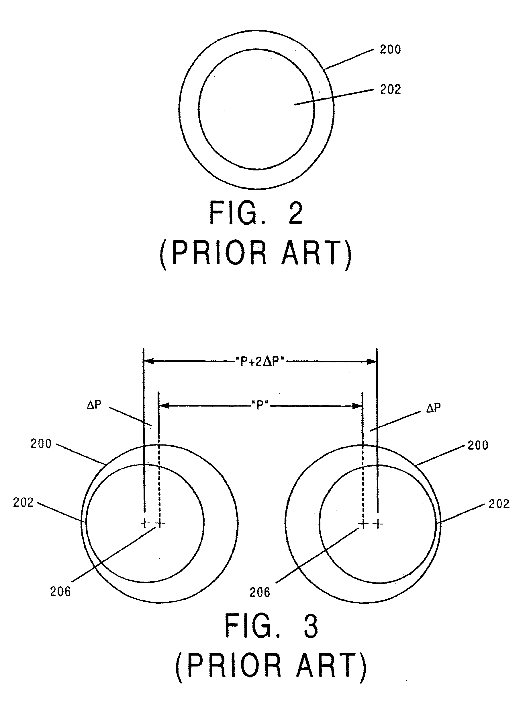
However, even if the center-to-center pitch of the holes is very accurate, because the hole diameter is larger than the fiber (and each hole likely varies across an array) each fiber need not be in the exact same place in the hole as the other fibers in their holes, then that can cause misalignment, leading to inefficiencies or unacceptable losses.
While this may be acceptable for multi-mode fibers, for single mode fibers this would be a huge offset that could make connections unacceptable or impossible.
Nevertheless, in actuality, the ferrule hole 200 must be larger than the fiber 202 by enough of a margin to allow for easy insertion—ultra-tight tolerances can not be effectively used.
Plastic molding technology is very process sensitive and molds having the requisite precision are extremely difficult to make.
Even so, yields tend to be poor due to the inherent manufacturing process errors that occur in plastics molding.
Since the tolerances on these pieces must be very accurate (on the order of about 1 to 2 micrometers), high yield manufacture is difficult.
As a result, the cost of terminating fiber bundles into these connectors can be quite expensive, running hundreds of dollars per side.
In addition, the process is not scalable to larger numbers of fibers (particularly 30 or more) because of inaccuracies and yield issues associated with molding technology and reliable production of ferrules for similar numbers of single mode fibers is even more difficult.
One manufacturer is known to have made a 5×12 connector array, but achieved such poor yields that they deemed an array of that size unmanufacturable.
Moreover, the cost of producing the pieces resulted in their being sold for $500 each, due to poor yield, and the mold for producing the pieces was destroyed during the process.
The problem is that in plastic molding pieces for holding higher fiber counts in small spaces results in less structural integrity for the molded piece.
As such, the prior art has been forced to do without commercial connectors for such large arrays, because 5×12 arrays can not be reliably created and commercial connectors for larger format arrays (e.g. even a 6×12) are considered prohibitively difficult to even attempt.
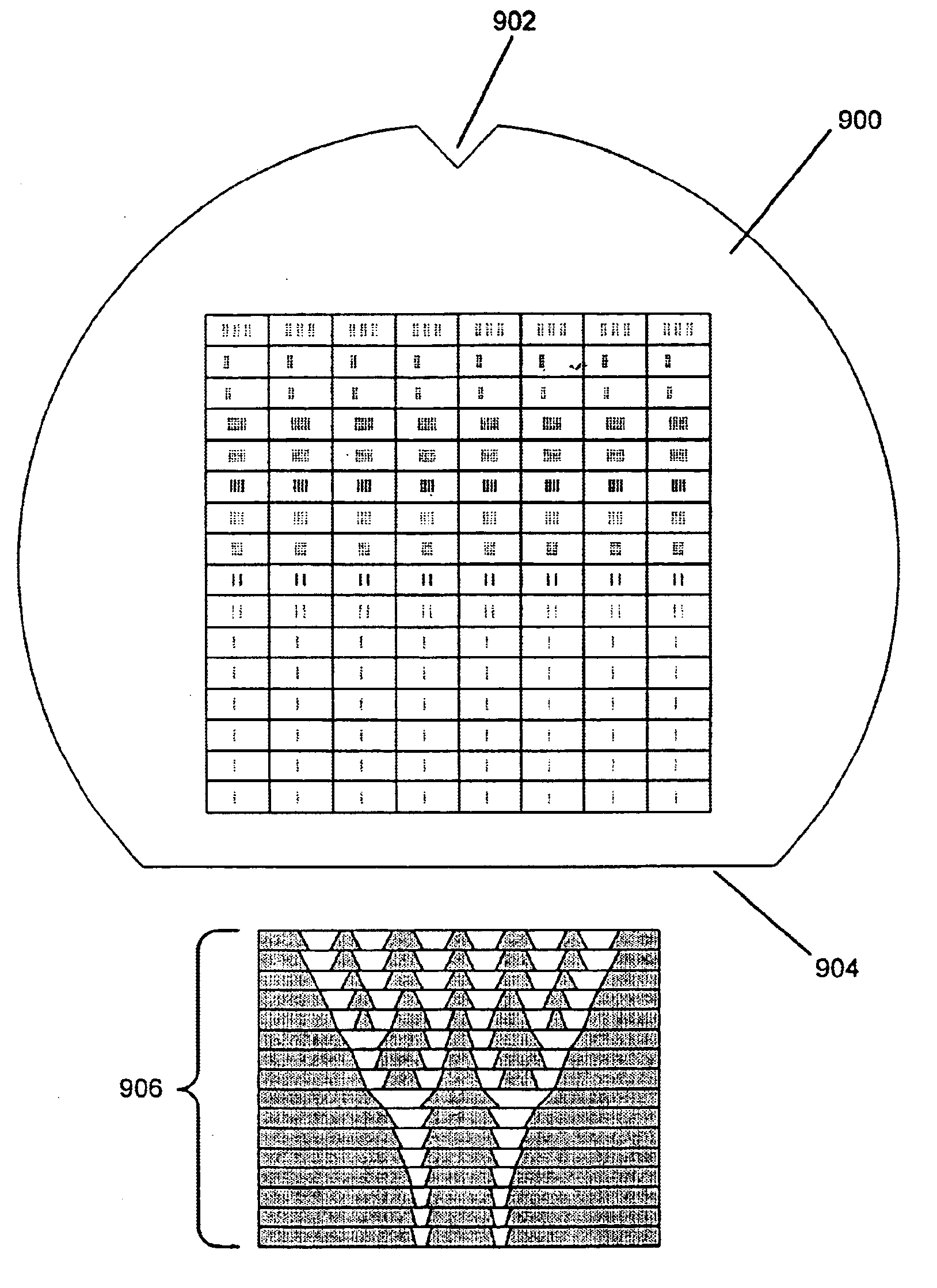
The ferrule area is very small, since ferrules for the above MTP, MPO, MPX or SMC connectors are about 0.07″ high, 0.3″ wide and 0.4″ deep, so molding or machining of features in the ferrules of the sizes required to hold multiple optical fibers (which typically have about a 125 micron diameter for a multimode fiber and a 9 micron diameter core for a single mode fiber) is very difficult.
Since single mode fibers have an even smaller diameter than multimode fibers, molding or machining ferrules to accommodate large arrays of single mode fibers is currently, for all practical purposes, impossible—particularly on a cost effective commercially viable scale.
Additionally, making ferrules for arrays is made more difficult due to process variations during production because, as the holes approach the edge of the ferrule, the structural integrity of the walls decrease causing parts to have poor tolerance at the periphery, become overly fragile causing component collapse in some cases, or prohibiting removal of material from the inside of the piece that impedes or prevents fiber insertion.
However, these attempts have not yielded a solution, particularly for the types of connectors mentioned above, because the inaccuracies of fiber production result in diameters of fibers which fluctuate within a 2 micron range (i.e. plus or minus 1 micron).
Even with multi-mode fibers (the best of which use 50 micron cores), a misalignment of 12 microns will cause unacceptable light loss for most applications.
For two-dimensional fiber arrays, the problem is even worse because the inaccuracy of the fiber is not limited to one direction.
Compounding the problem is the further fact that fiber inaccuracies stated as plus or minus 1 micron do not mean that fiber manufacturers guarantee that the fiber will be inaccurate by no more than 1 micron.
This means that most of the fiber should only be that inaccurate.
As a result, the larger the number of fibers, the more likely a problem due to fiber inaccuracy will occur because, for example, using the 16×16 array above, the array would have 256 times the chance (because there are 16×16=256 fibers) of having at least one of these statistically anomalous fibers in the group.
Others have attempted to align two dimensional arrays of fibers (e.g. 4×4 arrays) in a research setting, but none have applied their techniques to conventional connector technologies.
Moreover, the techniques are not suitable or readily adaptable for high yield, low cost, mass production as demanded by the industry.
The approach used the silicon pieces to hold the fibers but no attempt was made to integrate such an arrangement into a commercial connector.
While these silicon pieces were able to hold fibers, they were not designed to be, and could not readily be, used with existing ferrule or connector technology.
Moreover, they could not be used for single mode fibers with any accuracy.
Thus, none of the above attempts have provided a viable solution to the problem of how to effectively create a large format fiber array which: allows for high precision holding of large arrays of fibers, especially single mode fibers, is compatible with current commercially used connectors that attach two fiber bundles to each other or one fiber bundle to a component containing an array of optical devices, such as lasers and / or detectors, and that allows for easy fiber termination in a rapid fashion at low production cost.
In addition, because of the above problems, there is presently no large format ferrule apparatus that can maintain fibers at a low angle, or at a precisely specified angle, for good optical coupling.
However, when dealing with optical communication systems, faceplates can not be used because the light loss resulting from such a collimating arrangement is significant.
The faceplate technique (sometimes also referred to as oversampling) is also incompatible with the use of single mode fibers or lasers (which are highly desirable for use in high speed, long distance data transmission).
Hence, the collimating technique of using a faceplate, such as made for use in cameras, is an unworkable approach for opto-electronic communication devices.
This is an operational approach for forming a one-dimensional array that is unsuitable for mass production.
Unfortunately, the accuracy of stacking in the second dimension is limited by the accuracy of the thickness of the individual wafers, both on an absolute basis and on a relative basis, due to thickness variations over the area of the wafer.
In addition, the stacked V-Groove technique requires such accuracy that individual stacks must be individually built up one at a time; a costly and inefficient process.

Method used


Image

  • Multi-piece fiber optic component and manufacturing technique
  • Multi-piece fiber optic component and manufacturing technique
  • Multi-piece fiber optic component and manufacturing technique

Examples


Embodiment Construction

Overview

[0077]In overview, the technique uses one or more high-precision pieces that can be combined with a low precision piece to form a ferrule-like unit and then integrated into a commercial connector as the ferrule the connector is designed to receive.

Low Precision Piece Creation

[0078]An example of a low-precision piece 500 is shown in FIG. 5. As shown, this particular shape piece is designed in the shape of a ferrule opening in an industry standard connector apparatus so it can be inserted into a commercial connector, for example, in place of the ferrule 102 of FIG. 1. In practice, this currently means the piece should typically be shaped to dimensionally fit into at least one of an MTP or MPO or MPX or SMC style connector. Depending upon the particular variant, the low-precision piece 500 is manufactured by, for example, a polymer molding technique, for example, injection molding, transfer molding, or by some other molding, milling or forming technique. In some variants, the m...


PUM


Abstract

An apparatus for use in a commercial fiber optic connector is made up of an assembly of a set of slices. Each of the slices having multiple through holes of a specified arrangement. At least some of the through holes on any two adjoining slices are aligned with respect to each other so as to define a conduit between them. A transmission medium is within the holes. A method of making a fiber optic connector adapted to receive a fiber bearing unit is also described. The method involves coupling at least two high precision pieces together, the at least two high precision pieces having holes configured with an optical medium inserted therein after the coupling and cured to form a waveguide structure, coupling the at least two high precision pieces to a low precision piece to form a unit, and housing the unit within a fiber optic connector housing.

Description

[0001]This is of co-pending application Ser. No. 09 / 896,196, filed Jun. 29, 2001.FIELD OF THE INVENTION[0002]This invention relates to components and processes for fiber optic related component fabrication. More particularly, the invention relates to fabrication of fiber optic connectors and components used in conjunction therewith.BACKGROUND OF THE INVENTION[0003]Optical Fibers in commercial systems have been traditionally held by using a combination of pieces.[0004]A connector assembly 100, such as shown in FIG. 1 as an exploded view is used to attach various fiber pieces (or fiber pieces and modules) together. A ferrule 102 is the part of the connector 100 into which the fibers 104 themselves are inserted before the ferrule 102 is inserted into the overall connector itself. The ferrule 102 is a ‘high-precision’ piece of the assembly 100. It holds the fiber(s) 104 in a precise position and ensures that when two connector pieces are attached, that the fibers in the two pieces are h...

Claims


Application Information

Patent Timeline
Patent Type & Authority Patents(United States)
IPC IPC(8): G02B6/36G02B6/38G02B6/42G02B6/32
CPCG02B6/4249G02B6/3834G02B6/3835G02B6/3885G02B6/32G02B6/3636G02B6/3644G02B6/3652G02B6/3672G02B6/3676G02B6/3696G02B6/3839G02B6/3692
Inventor TREZZA, JOHNKANG, KEITHDUDOFF, GREGOLSON, RONALD
Owner CUFER ASSET LTD LLC
Why Eureka
Try Eureka