Adjustable hyperspectral detection chip enhanced by multi-resonance plasmonic mechanism

a plasmonic mechanism and hyperspectral detection technology, applied in the field of infrared detectors, can solve the problems of difficult chipization and integration, limited detection wavelength of existing conventional infrared photodetectors, and inability to detect longer bands, etc., to achieve the effect of reducing the bandwidth of the optical absorption spectrum of the infrared detection chip, and reducing the spectral resolution

Active Publication Date: 2021-07-13
SOUTHEAST UNIV
View PDF55 Cites 0 Cited by
  • Summary
  • Abstract
  • Description
  • Claims
  • Application Information

AI Technical Summary

Benefits of technology

[0005]Technical Problem: An objective of the present invention is to resolve the technical problems of existing infrared photodetectors such as that a detection wavelength is limited by a semiconductor band gap, a detection range is limited, the quantum efficiency is low, spectral resolution is low, and it is difficult to achieve integration and large-scale chipization by using discrete devices, and provide an adjustable hyperspectral detection chip enhanced by a multi-resonance plasmonic mechanism. A heterojunction is formed by using a metal nanonail and a semiconductor to achieve optical detection that breaks through the cut-off wavelength of the semiconductor based on plasmonic resonance enhanced hot carrier effect. Narrowing of the bandwidth of the optical absorption spectrum caused by competition between two, horizontal and vertical, resonance modes of the metal nanonail is utilized, and when the metal nanonail is added to the infrared photodetector, local light intensity density of light incident on a detection material can be increased to significantly improve the quantum efficiency of the detector material. A plasmonic resonance using plasmonic nanoparticles is related to a refractive index of a surrounding medium. Nanonails are loaded inside the control material layer, and a distribution state of the control material layer is changed by using a external control signal, and the refractive index of the medium surrounding the nanonails is changed, to achieve real-time control of the peak position of a detector response spectral band, and spectral resolution is better than 1 nanometer. The detection chip has advantages such as an extendable detection wavelength, high the quantum efficiency, high spectral resolution, integration, low costs, and a simple fabrication process, and can be used to fabricate an arrayed hyperspectral detector.
[0012]The nanonail array is formed by structures of plasmonic nanonails with a multi-resonance enhancement effect arranged periodically, and the plasmonic nanonail with the multi-resonance enhancement effect includes two parts: a triangular nanoplate and a nanorod, and the plasmonic nanonail with the multi-resonance enhancement effect has characteristics of infrared ultra-narrow band absorption, strong short-range dielectric sensitivity, and strong polarization selectivity.
[0017]Advantageous Effect: Compared with the prior art, the present invention has the following advantages:
[0018]1. An adjustable hyperspectral detection chip enhanced by a multi-resonance plasmonic mechanism is provided. By utilizing characteristics of ultra-narrow band infrared light absorption, polarization selection, and sub-wavelength light control of a plasmonic nanonail structure with a multi-resonance enhancement effect, multi-function monolithic integration of hyperspectral detection, polarization detection, and diffraction limit breakthrough detection is implemented, and a problem that a conventional infrared photodetector performs light splitting and polarization selection by using discrete devices, and cannot implement integration of a high-performance detection system is overcome.
[0019]2. An adjustable hyperspectral detection chip enhanced by a multi-resonance plasmonic mechanism is provided. By utilizing strong ultra-narrow band absorption of a plasmonic nanonail structure with a multi-resonance enhancement effect and strong sensitivity of a resonance peak thereof to a short-range dielectric environment, hyperspectral detection of an infrared band photo-induced hot carrier mechanism is implemented, so that a problem that spectral resolution of an existing infrared optoelectronic detection chip is low can be overcome, and spectral resolution is better than 1 nanometer.
[0020]3. An adjustable hyperspectral detection chip enhanced by a multi-resonance plasmonic mechanism is provided. By utilizing a mechanism of competition between two, horizontal and vertical, resonance modes of a nanonail, the bandwidth of the optical absorption spectrum of an infrared detection chip is greatly narrowed, and after a metal nanonail multi-resonance plasmonic structure is added to an infrared photodetector, local light intensity density of light incident on a detection material can be increased by 2-4 orders of magnitude to significantly improve the quantum efficiency of the detector.

Problems solved by technology

However, detection wavelengths of the existing conventional infrared photodetectors are limited by a band gap of a semiconductor material and a longer band cannot be detected.
In addition, a photodetector usually performs light spitting on infrared radiation by using discrete devices such as a prism, a grating, or distributed Bragg reflectors, to achieve infrared multi-spectral imaging, but it is difficult to achieve chipization and integration.

Method used


Image

  • Adjustable hyperspectral detection chip enhanced by multi-resonance plasmonic mechanism
  • Adjustable hyperspectral detection chip enhanced by multi-resonance plasmonic mechanism
  • Adjustable hyperspectral detection chip enhanced by multi-resonance plasmonic mechanism

Examples


embodiment

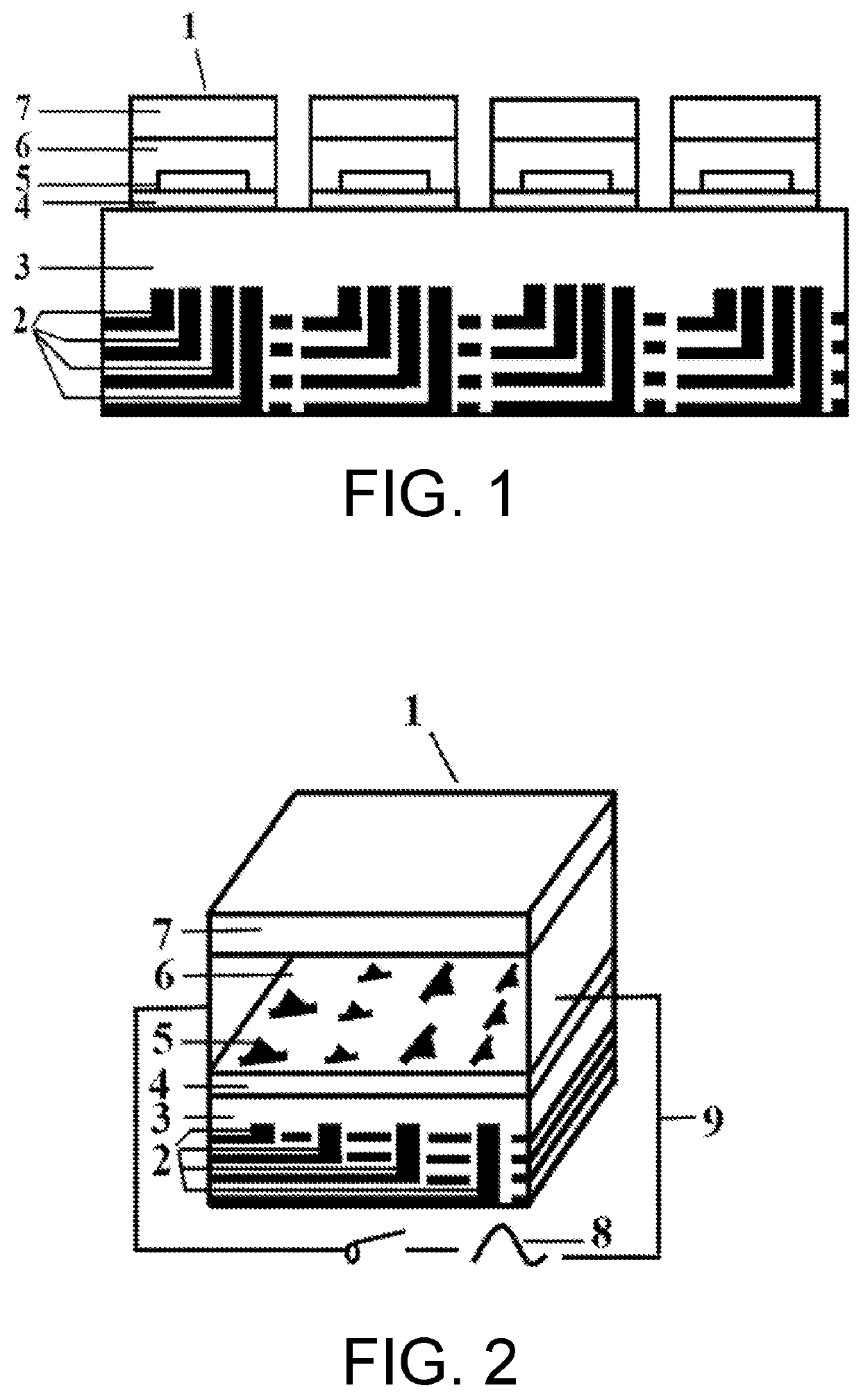
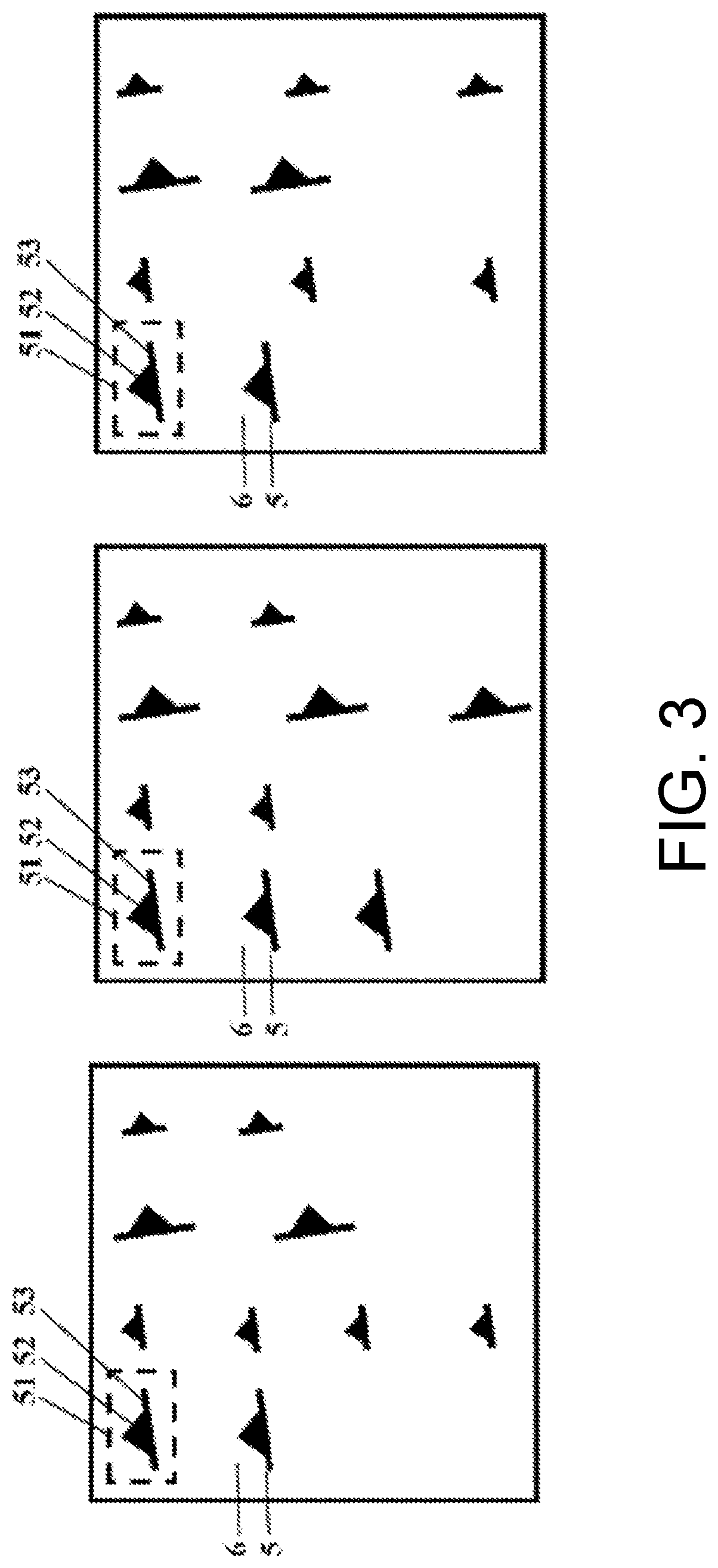
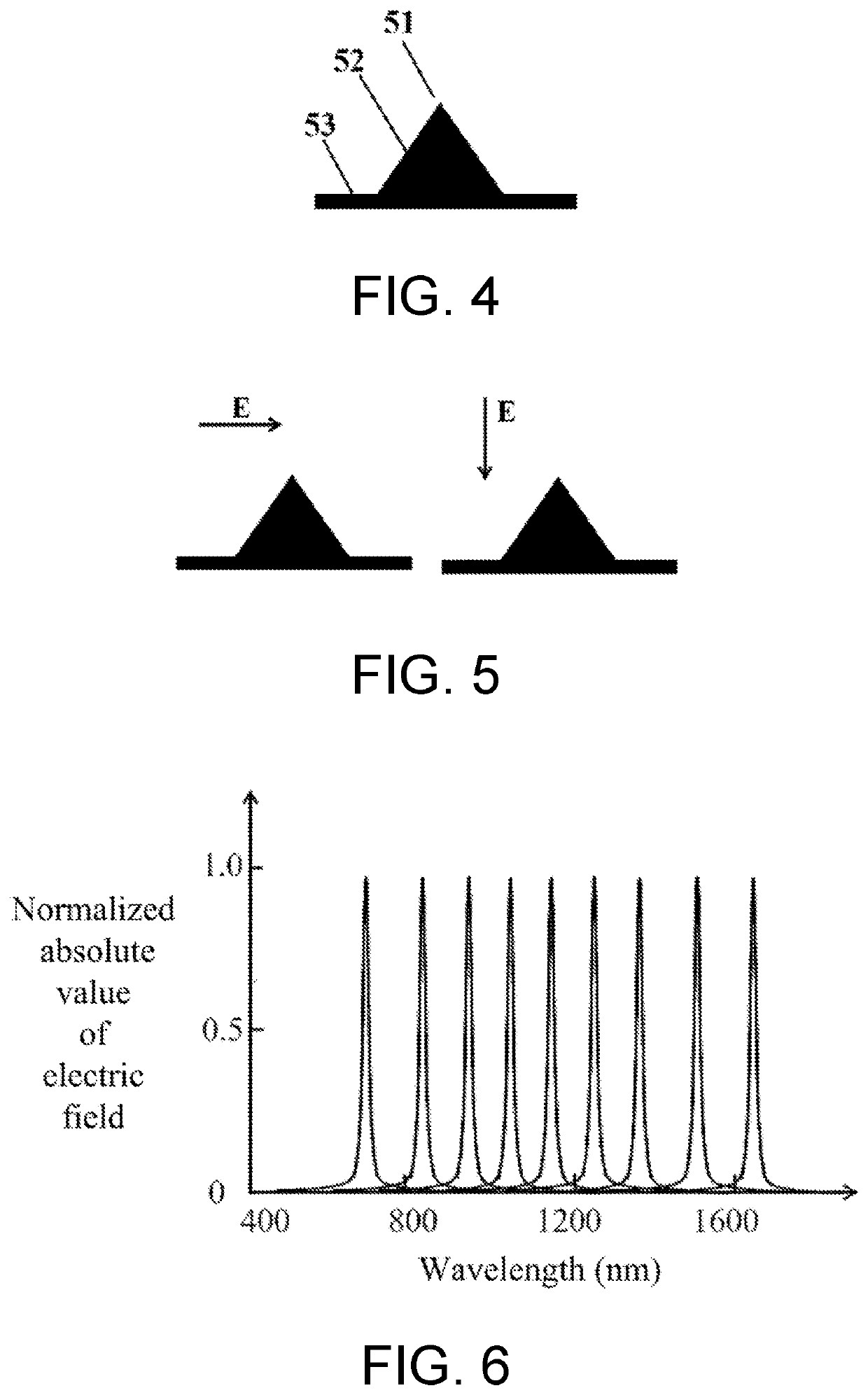
[0036]A detection unit structure of an adjustable hyperspectral detection chip enhanced by a multi-resonance plasmonic mechanism is shown in FIG. 1, including an aluminum electrode 2, an n-type silicon 3, a silicon-dioxide layer4, a silver nanonail array 5, an electro-optical control material layer 6, an indium tin oxide electrode 7, a periodical voltage control signal 8, and a driving circuit 9. The silver nanonail array 5 is loaded inside the electro-optical control material layer 6. The silver nanonail array 5 is formed by silver nanonails 51 arranged periodically, and the silver nanonail 51 includes two parts: a silver triangular nanoplate 52 and a silver nanorod 53, and the driving circuit 9 is connected to both sides of the control material layer 6.

[0037]When light is irradiated on the detection unit, carriers cross the Schottky barrier to form a photocurrent by using a heterojunction between the n-type silicon 3 and the silver nanonail array 5 based on a plasmon-induced hot c...


PUM

PropertyMeasurementUnit
sizeaaaaaaaaaa
sizeaaaaaaaaaa
sizeaaaaaaaaaa

Abstract

An adjustable hyperspectral detection chip enhanced by a multi-resonance plasmonic mechanism. The detection chip consists of an array of metal nanonail resonator detection units. Each detection unit (1) comprises: a bottom electrode (2), a semiconductor material layer (3), a spacer layer (4), a nanonail array (5), a control material layer (6), a top electrode (7), a peripheral control signal (8), and a driving circuit (9). The positional relationship from top to bottom is the top electrode (7), the control material layer (6), the nanonail array (5), the spacer layer (4), the semiconductor material layer (3), and the bottom electrode (2). The nanonail array (5) is loaded inside the control material layer (6), and the peripheral control signal (8) and the driving circuit (9) are connected to both sides of the control material layer (6).

Description

CROSS-REFERENCE TO RELATED APPLICATION[0001]This application is a continuation of international PCT application serial no. PCT / CN2018 / 088736, filed on May 25, 2018, which claims the priority benefit of Chinese application no. 201810171259.0, filed on Mar. 1, 2018. The entirety of each of the above-mentioned patent applications is hereby incorporated by reference herein and made a part of this specification.BACKGROUNDTechnical Field[0002]The present invention belongs to the fields such as the field of infrared detectors and the field of metal nanomaterials, and specifically, to an adjustable hyperspectral detection chip enhanced by a multi-resonance plasmonic mechanism.Description of Related Art[0003]In the hyperspectral imaging detection technology, a hyperspectral image with specific spectral resolution is used for target detection. Compared with the conventional single-wide band optoelectronic detection technology, the hyperspectral imaging detection technology requires a combinat...

Claims


Application Information

Patent Timeline
Patent Type & Authority Patents(United States)
IPC IPC(8): G01J3/447G01J3/28H01L27/146H01L31/0232H01L31/0352H01L31/101
CPCG01J3/447G01J3/2823H01L27/14625H01L31/02327H01L31/0352H01L31/1013G01J2003/2826H01L27/14601H01L27/14649H01L31/108
Inventor ZHANG, TONGSU, DANXIONG, MENGSHAN, FENGZHANG, XIAOYANG
Owner SOUTHEAST UNIV
Why Eureka
Try Eureka