On-chip IEC ESD protection using parasitic PNP devices

a technology of parasitic pnp and on-chip iec, which is applied in the direction of semiconductor devices, electrical equipment, transistors, etc., can solve the problems of high requirements for system-level esd design, difficult on-chip esd protection for high-speed interface ics, and large chip area of on-chip iec esd protection structures, etc., to improve the robustness and reliability of circuit design, and avoid series resistance

Active Publication Date: 2021-08-17
THE BOARD OF TRUSTEES OF THE UNIV OF ARKANSAS
View PDF8 Cites 0 Cited by
  • Summary
  • Abstract
  • Description
  • Claims
  • Application Information

AI Technical Summary

Benefits of technology

[0009]In one embodiment, the present invention provides a method, system, approach and solution that provide ESD protection for high-speed interface ICs (e.g., USB host controller ICs) that require both IC-level (e.g., HBM) and system-level (e.g., IEC) ESD protections due to system exposures to static electricity discharges. On-chip ESD protection for high-speed interface ICs is difficult due to the stringent pin requirements (i.e., low capacitance and no series resistance). Specifically, the ESD designs for system-level ESD requirements are more challenging because of the high discharge current (˜30 A), limited type of ESD components and narrow protection window. Although system-level stress that reaches ICs will vary according to the board-level components and PCB layout, on-chip IEC ESD protection structures typically require a tremendous amount of chip area (e.g., over 0.2 mm2). Therefore, area-efficient IEC ESD and low-capacitance HBM ESD protection for high-speed interface ICs are highly desired to improve the robustness and reliability of the circuit design.
[0010]In other embodiments, the present invention provides innovative approaches that utilize parasitic components in the widely-used dual-diodes ESD protection structures in high-speed interface ICs. Area-efficient robust dual-diode structures can be integrated with different types of primary ESD cells other than SCR devices to reduce the impacts to the circuit performance and meet specific pin requirements.
[0012]In other embodiments, the present invention provides a protection structure wherein the structure is implemented in high-speed or digital designs due to small capacitance and low leakage current.
[0013]In other embodiments, the present invention provides a protection structure of wherein the structure is integrated with different types of primary ESD cells other than SCR devices to reduce the impacts to the circuit performance and meet specific pin requirements.
[0016]In other embodiments, the present invention provides a protection structure of wherein the current gain of the parasitic PNP structures can be adjusted through varying the width and doping for the emitter and base.

Problems solved by technology

On-chip ESD protection for high-speed interface ICs is difficult due to the stringent pin requirements (i.e., low capacitance and no series resistance).
Specifically, the ESD designs for system-level ESD requirements are more challenging because of the high discharge current (˜30 A), limited type of ESD components and narrow protection window.
Although system-level stress that reaches ICs will vary according to the board-level components and PCB layout, on-chip IEC ESD protection structures typically require a tremendous amount of chip area (e.g., over 0.2 mm2).

Method used


Image

  • On-chip IEC ESD protection using parasitic PNP devices
  • On-chip IEC ESD protection using parasitic PNP devices
  • On-chip IEC ESD protection using parasitic PNP devices

Examples


Embodiment Construction

[0031]Detailed embodiments of the present invention are disclosed herein; however, it is to be understood that the disclosed embodiments are merely exemplary of the invention, which may be embodied in various forms. Therefore, specific structural and functional details disclosed herein are not to be interpreted as limiting, but merely as a representative basis for teaching one skilled in the art to variously employ the present invention in virtually any appropriately detailed method, structure or system. Further, the terms and phrases used herein are not intended to be limiting, but rather to provide an understandable description of the invention.

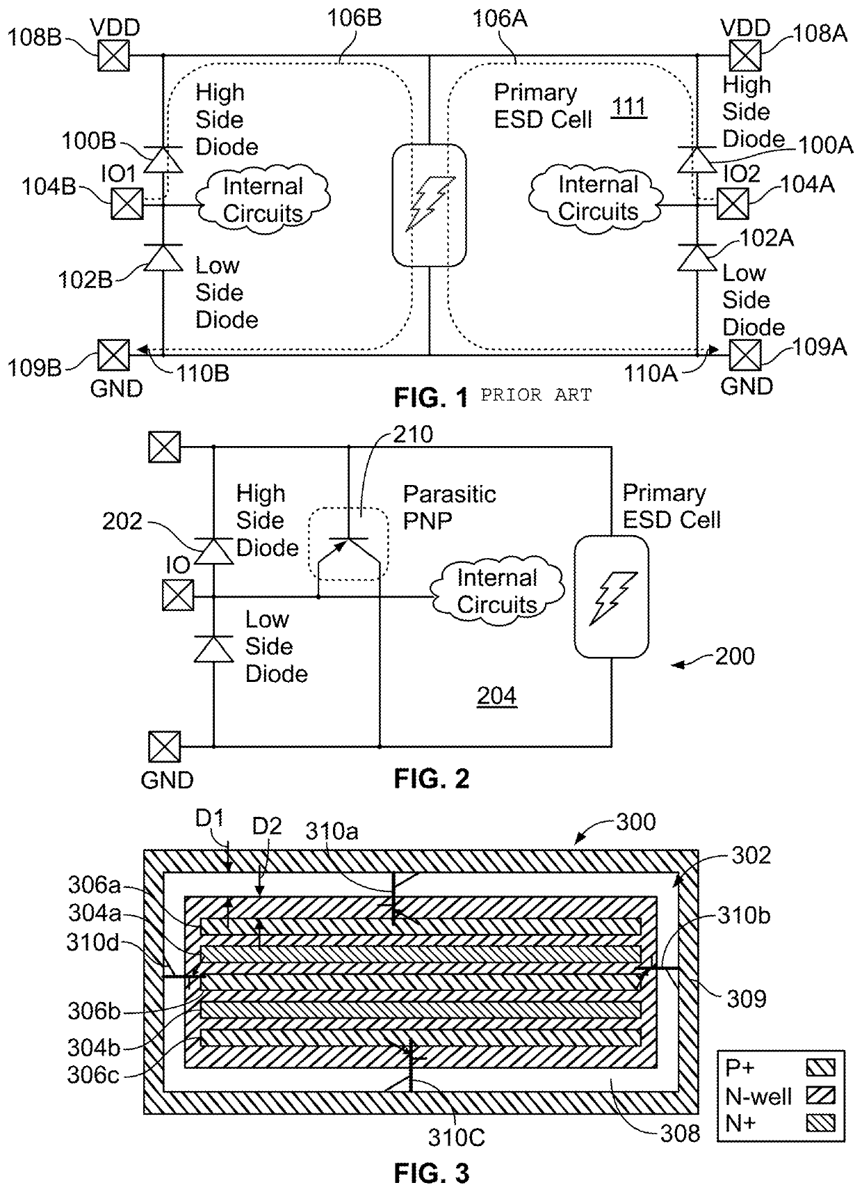
[0032]In one embodiment, as shown in FIG. 2, the present invention proposes a novel area-efficient rail-based ESD protection structure 200 by utilizing a parasitic bipolar structure formed between the high-side ESD diode 202 and the chip substrate 204. In another embodiment, the rail-based ESD protection may be used in a number of semicondu...


PUM

PropertyMeasurementUnit
currentaaaaaaaaaa
currentaaaaaaaaaa
currentaaaaaaaaaa

Abstract

A semiconductor device having a P type substrate, an N type layer on the P type substrate that forms a PN junction therewith and the P type region, N type region and P type substrate form at least one parasitic PNP transistor.

Description

RELATED APPLICATIONS[0001]This application claims priority to U.S. Provisional Application Ser. No. 62 / 735,762 filed Sep. 24, 2019, and is hereby incorporated herein by reference in its entirety.STATEMENT REGARDING FEDERALLY SPONSORED RESEARCH & DEVELOPMENT[0002]Not applicable.INCORPORATION BY REFERENCE OF MATERIAL SUBMITTED ON A COMPACT DISC[0003]Not applicable.BACKGROUND OF THE INVENTION[0004]Electrostatic discharge (ESD) has been identified as one of the most significant reliability issues to ICs and systems. IC-level ESD standards (e.g., Human Body Model and Charge Device Model (CDM)) are used to determine the sensitivity of components and integrated circuits to degradation or damage under the ESD conditions during human or machine handling, System-level ESD tests (e.g., IEC 61000-4-2, IS0106056) are defined to assess the robustness of end-user products to ESD events that can occur during product operations. Although system-level ESD tests are not typically intended to be applie...

Claims


Application Information

Patent Timeline
Patent Type & Authority Patents(United States)
IPC IPC(8): H01L27/02
CPCH01L27/0262H01L27/0259
Inventor CHEN, ZHONGFARBIZ, FARZAN
Owner THE BOARD OF TRUSTEES OF THE UNIV OF ARKANSAS
Why Eureka
Try Eureka