Organic light emitting diode display device and method of fabricating the same

a light-emitting diode and display device technology, applied in semiconductor devices, semiconductor/solid-state device testing/measurement, instruments, etc., can solve problems such as difficulty in accurate control of a disposition place and fine adjustment of an amoun

Active Publication Date: 2021-08-17
LG DISPLAY CO LTD
View PDF9 Cites 0 Cited by
  • Summary
  • Abstract
  • Description
  • Claims
  • Application Information

AI Technical Summary

Benefits of technology

[0007]An aspect of the present disclosure is to provide an organic light emitting diode display device where an error in a deposition position during a deposition process of a light emitting layer is minimized or reduced, and a method of fabricating the organic light emitting diode display device.
[0008]Another aspect of the present disclosure is to provide an organic light emitting diode display device where an error in a deposition range of a light emitting layer during a deposition process of the light emitting layer is minimized or reduced, and a method of fabricating the organic light emitting diode display device.

Problems solved by technology

However, during the disposition process, there exists difficulties in accurate control of a disposition place and a fine adjustment of an disposition amount.

Method used


Image

  • Organic light emitting diode display device and method of fabricating the same
  • Organic light emitting diode display device and method of fabricating the same
  • Organic light emitting diode display device and method of fabricating the same

Examples


first embodiment

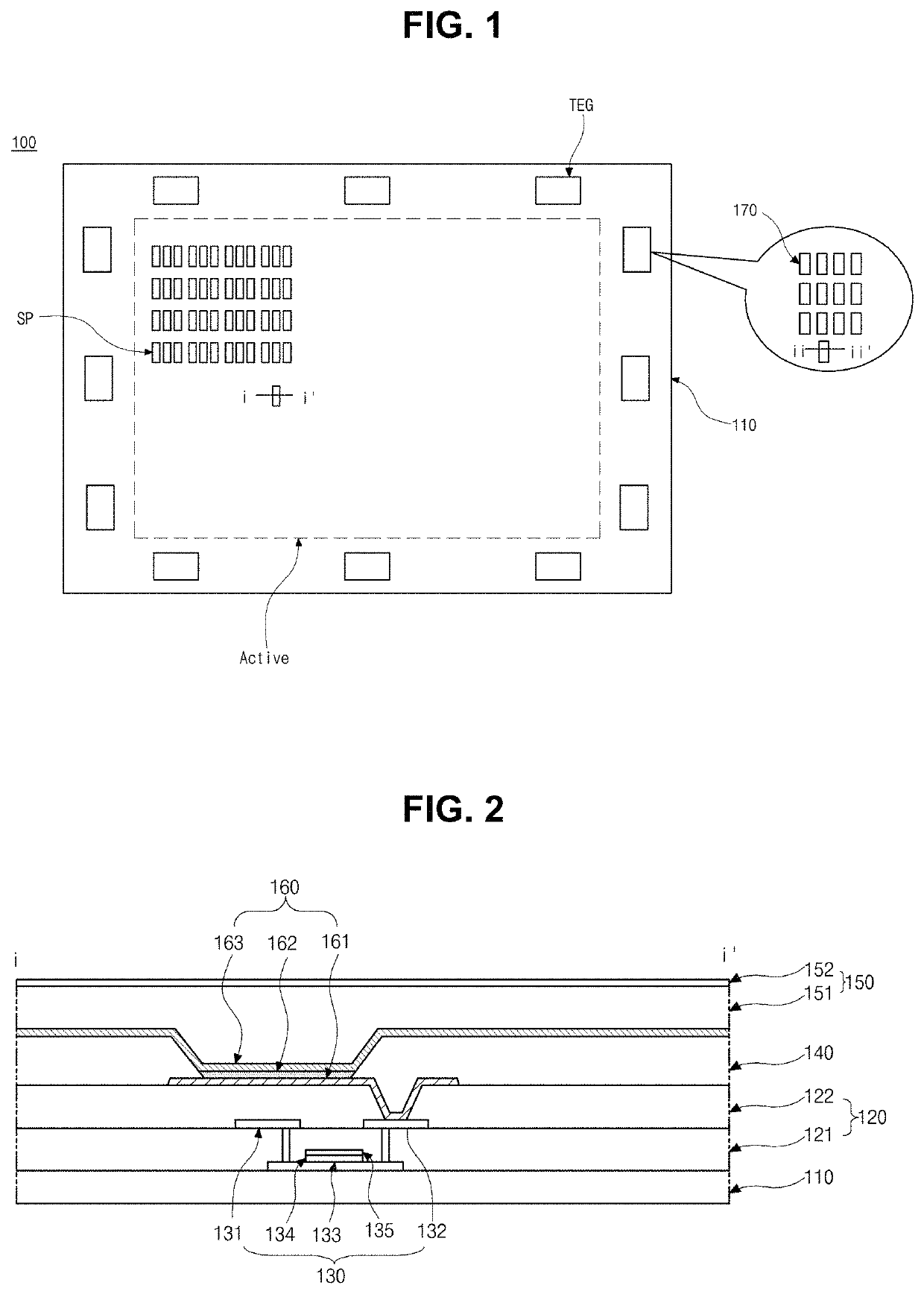
[0037]FIG. 1 is a plan view showing an organic light emitting diode display device according to the present disclosure.

[0038]In FIG. 1, an organic light emitting diode (OLED) display device 100 includes a substrate 110 having a plurality of pixels SP. The substrate 110 includes at least one test element group TEG (TEG: Test Element Group, Test pattern Element Group) having a dummy pattern 170. The substrate 110 may be a glass substrate or a flexible substrate of a polyimide group. In addition, the substrate may have a multiple structure including a barrier layer for minimizing or reducing infiltration of moisture and oxygen.

[0039]Although not shown, the at least one test element group TEG may include an additional driving element connected to the dummy pattern 170 and a circuit unit for applying a current.

[0040]The pixel SP is disposed in an display region on the substrate 110, and the at least one test element group TEG may be disposed in a non-display region surrounding the displa...

second embodiment

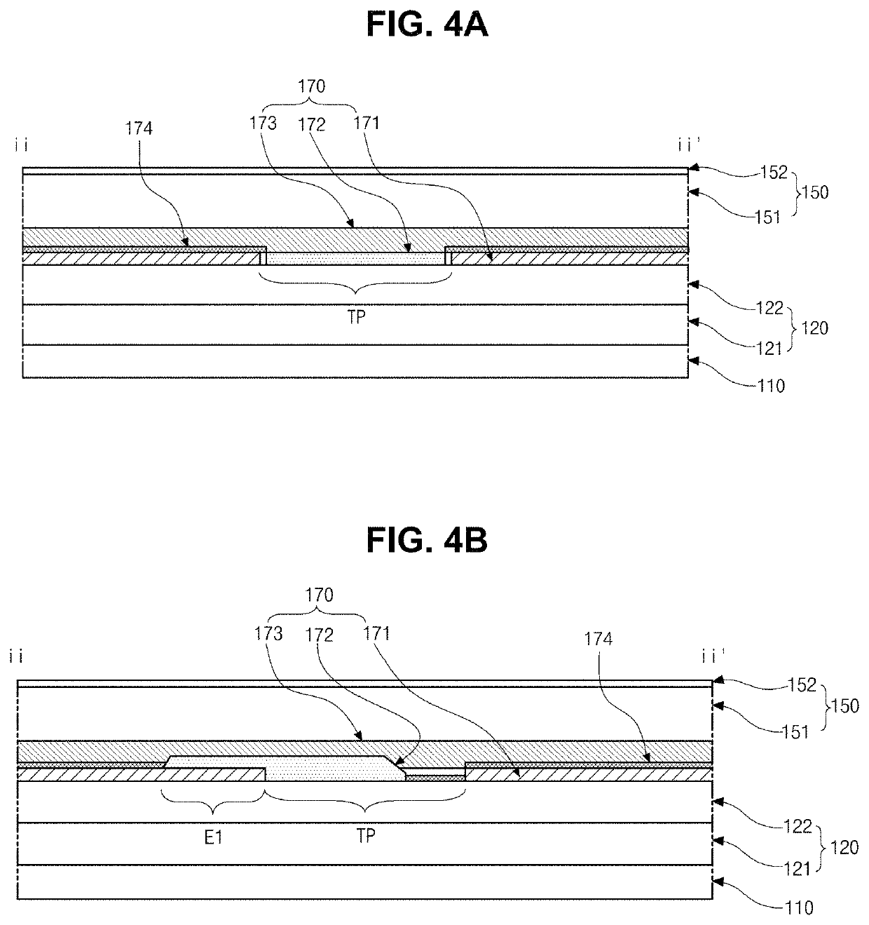
[0077]FIG. 5C is a cross-sectional view showing a disposition error of a light emitting layer of an organic light emitting diode display device according to the present disclosure.

[0078]In FIG. 5C, although the dummy layer 172 of the dummy pattern 170 is designed not to overlap the verification portion TP and not to be electrically connected to the first electrode 171, an error such that the dummy layer 172 is disposed to overlap the first electrode 171 in a third error portion E3 may occur due to the disposition error of the light emitting layer 162. As a result, the first and second electrodes 171 and 173 may be electrically connected to each other through the dummy layer 172 of the dummy pattern 170 in the third error portion E3.

[0079]When the hole and the electron are injected into the dummy layer 172 of the dummy pattern 170 in the third error portion E3 through the first and second electrodes 171 and 173, respectively, the hole and the electron are recombined in an emitting ma...


PUM

PropertyMeasurementUnit
peak wavelength rangeaaaaaaaaaa
difference distancesaaaaaaaaaa
currentaaaaaaaaaa

Abstract

An organic light emitting diode display device includes a substrate; a plurality of driving elements and a plurality of light emitting diodes on the substrate; and at least one dummy pattern on the substrate and including a first electrode, a dummy layer, and a second electrode, wherein the first electrode and the dummy layer are electrically separated from each other.

Description

CROSS REFERENCE TO RELATED APPLICATIONS[0001]The present application claims the priority benefit of Korean Patent Application No. 10-2018-0163437 filed in Republic of Korea on Dec. 17, 2018, which is hereby incorporated by reference in its entirety for all purposes as if fully set forth herein.BACKGROUNDTechnical Field[0002]The present disclosure relates to an organic light emitting diode display device, and more particularly, to an organic light emitting diode display device where a fabrication stability in a disposition of a light emitting layer and a method of fabricating the organic light emitting diode display device.Discussion of the Related Art[0003]An organic light emitting diode (OLED) display device is an emissive type display device. Because the OLED display device does not include a separate light source, the OLED display device has a light weight and a thin profile differently from a liquid crystal display (LCD) device. In addition, the OLED display device has an advant...

Claims


Application Information

Patent Timeline
Patent Type & Authority Patents(United States)
IPC IPC(8): H01L51/52H01L27/32H01L51/00H01L51/56
CPCH01L27/3223H01L27/3244H01L51/0031H01L51/56H01L22/12H01L22/34G09G3/006H10K59/88H10K59/12H10K59/1201H10K71/70H10K59/00H10K50/805H10K71/00
Inventor MUN, BYUNG-JUNELEE, SEUNG-HYUN
Owner LG DISPLAY CO LTD
Why Eureka
Try Eureka