OLED pixel driving circuit, array substrate and display device

a technology of organic light-emitting diodes and driving circuits, applied in the field of display technologies, can solve the problems of shortening the life of the oled, increasing the threshold voltage of the oled continuously, and continuing to decrease, so as to reduce the number of parasitic capacitors and data lines in the panel, the aperture ratio of the oled device is increased, and the light-emitting time of the oled is reduced

Active Publication Date: 2021-11-16
SHENZHEN CHINA STAR OPTOELECTRONICS SEMICON DISPLAY TECH CO LTD
View PDF8 Cites 2 Cited by
  • Summary
  • Abstract
  • Description
  • Claims
  • Application Information

AI Technical Summary

Benefits of technology

[0005]A technical problem mainly solved by the present invention is to provide an organic light emitting diode (OLED) pixel driving circuit, an array substrate, and a display device, which can reduce a number of parasitic capacitances and data lines in a panel and improve an aperture ratio of an OLED device.
[0015]Beneficial effects of the present invention are that: Different from the situation of the prior art, the present invention allows two OLEDs to share a driving thin film transistor, a storage capacitor, and a data line, so that the two OLEDs alternately emit light. In this way, the light emitting time of the OLEDs is reduced, the number of parasitic capacitors and data lines in a panel is reduced, and the aperture ratio of the OLED device is increased; and the OLEDs are enabled to be in reverse bias in a non-light emitting display frame, so that the OLEDs do not have to be in a DC bias state for a long time, and thus, the aging of the OLED device is slowed down. In addition, no other reverse bias voltage is connected externally, so the difficulty of tracing of the pixel circuit and the crosstalk from a bias voltage line to other signal lines are reduced.

Problems solved by technology

This causes a threshold voltage of the OLED to increase continuously, and luminous brightness of the OLED continues to decrease, and long-term light emission will shorten a life of the OLED and accelerate aging of the OLED.
Moreover, each OLED corresponds to a driving thin film transistor and a storage capacitor, which doubles a number of storage capacitors in the panel, resulting in an increase in parasitic capacitance of the panel.

Method used


Image

  • OLED pixel driving circuit, array substrate and display device
  • OLED pixel driving circuit, array substrate and display device
  • OLED pixel driving circuit, array substrate and display device

Examples


Embodiment Construction

[0019]The technical solutions in the embodiments of the present invention will be clearly and completely described below with reference to the accompanying drawings in the embodiments of the present invention. Obviously, the described embodiments are only a part of the embodiments of the present invention, but not all the embodiments. Based on the embodiments of the present invention, all other embodiments obtained by a person of ordinary skill in the art without making creative efforts shall fall within the protection scope of the present invention.

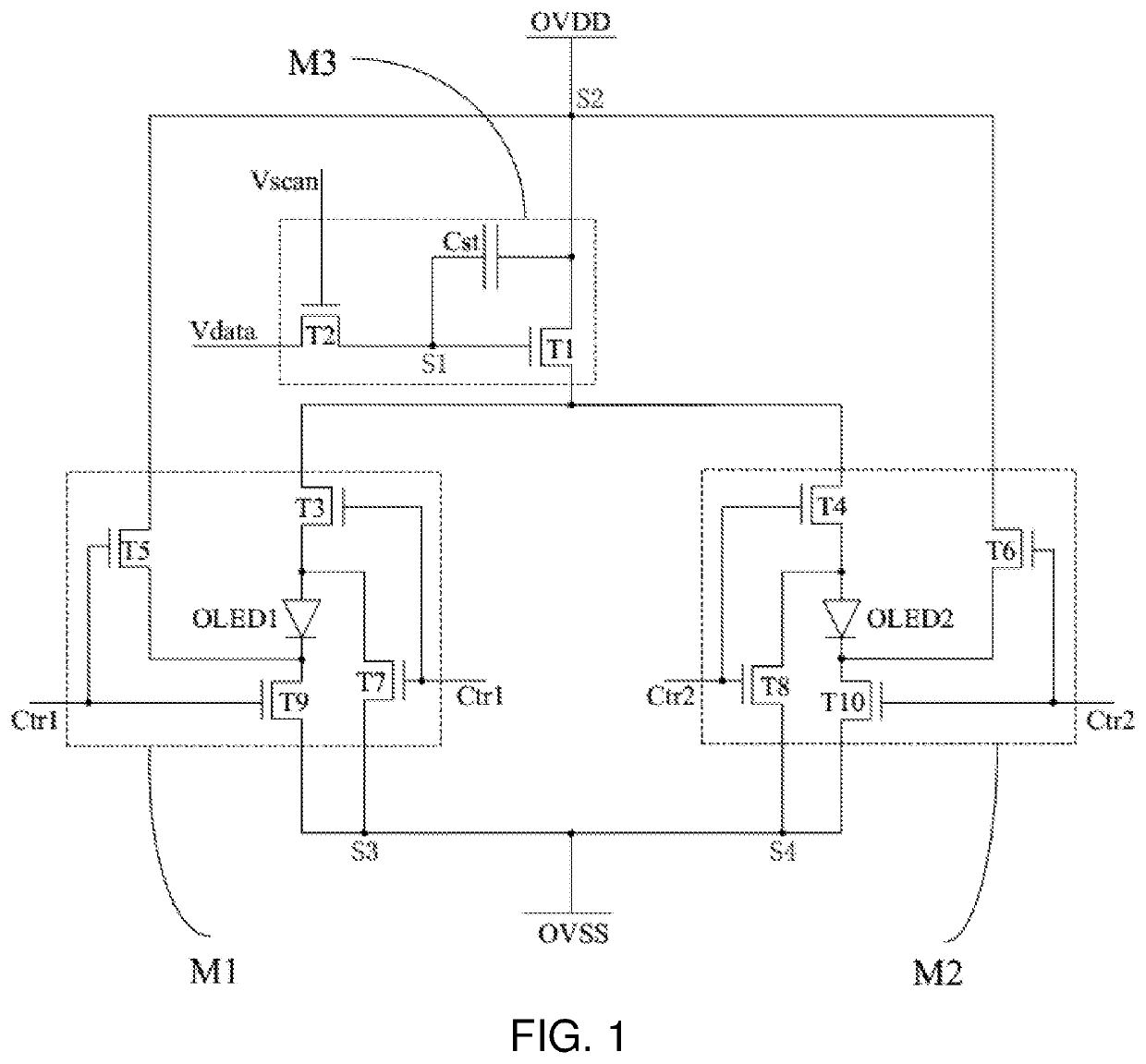
[0020]FIG. 1 is a schematic diagram of a specific structure of an OLED pixel driving circuit according to an embodiment of the present invention. The pixel driving circuit provided in this embodiment includes a driving control unit M3, a first light emitting unit M1, and a second light emitting unit M2. The driving control unit M3 includes a first switch T1, a second switch T2, and a storage capacitor Cst. A control end of the second swi...


PUM

PropertyMeasurementUnit
voltageaaaaaaaaaa
polarityaaaaaaaaaa
voltageaaaaaaaaaa

Abstract

OLED pixel driving circuit, array substrate and display device are provided. The pixel driving circuit comprises a driving control unit, a first light emitting unit and a second light emitting unit. Two OLEDs share one driving control unit, so the two OLEDs alternately emit light. In this way, light emitting time of the OLEDs is reduced, number of parasitic capacitors and data lines in a panel is reduced, and aperture ratio of the OLED device is increased; and OLEDs are enabled to be in reverse bias in a non-light emitting display frame, so that OLEDs do not have to be in a DC bias state for a long time, and thus, aging of the OLED device is slowed down. No other reverse bias voltage is connected externally, difficulty of tracing of the pixel circuit and crosstalk from a bias voltage line to other signal lines are reduced.

Description

FIELD OF INVENTION[0001]The present disclosure relates to the field of display technologies, and more particularly to an organic light emitting diode (OLED) pixel driving circuit, an array substrate, and a display device.BACKGROUND OF INVENTION[0002]Organic light emitting diodes (OLEDs) have many excellent characteristics such as wide color gamut, high contrast, and solid-state devices, so they are becoming more and more competitive in the field of display technology. Generally, a pixel array composed of electronic pixels is provided in a display area of an organic light emitting display, and each pixel unit includes a pixel driving circuit.[0003]Traditional 2T1C architecture circuit means that the circuit includes two thin film transistors and a storage capacitor. The thin film transistor that functions as a switch connects a data voltage to a gate of a driving thin film transistor when it is in the on state, and stores the data voltage on the storage capacitor. This keeps the driv...

Claims


Application Information

Patent Timeline
Patent Type & Authority Patents(United States)
IPC IPC(8): G09G3/325G09G3/3291G09G3/3266G09G3/36
CPCG09G3/325G09G3/3266G09G3/3291G09G3/3659G09G3/3258G09G3/3233G09G2300/0804G09G2300/0819G09G2300/0842G09G2300/0861G09G2310/0256G09G2320/045
Inventor CHANG, BOBIAOCHEN, XIAOLONGWEN, YI-CHIEN
Owner SHENZHEN CHINA STAR OPTOELECTRONICS SEMICON DISPLAY TECH CO LTD
Why Eureka
Try Eureka