

Direct type backlight device
a backlight device and direct type technology, applied in the field of backlight devices, can solve the problems of increasing the thickness of the lcd device, reducing the luminous efficiency of the light reflector, so as to achieve the effect of reducing the thickness of the light reflector and increasing the luminous efficiency of the direct type backlight devi
- Summary
- Abstract
- Description
- Claims
- Application Information
AI Technical Summary
Benefits of technology
Problems solved by technology
Method used
Image

Examples
first embodiment
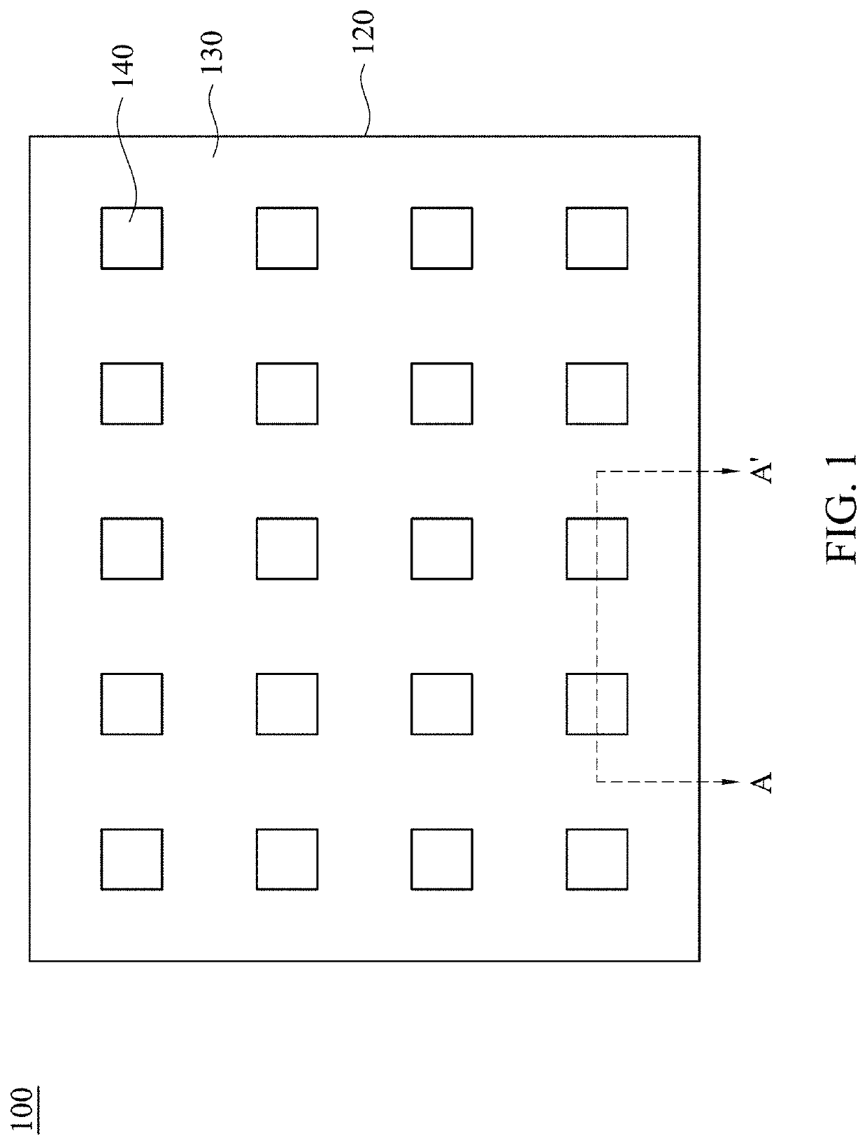
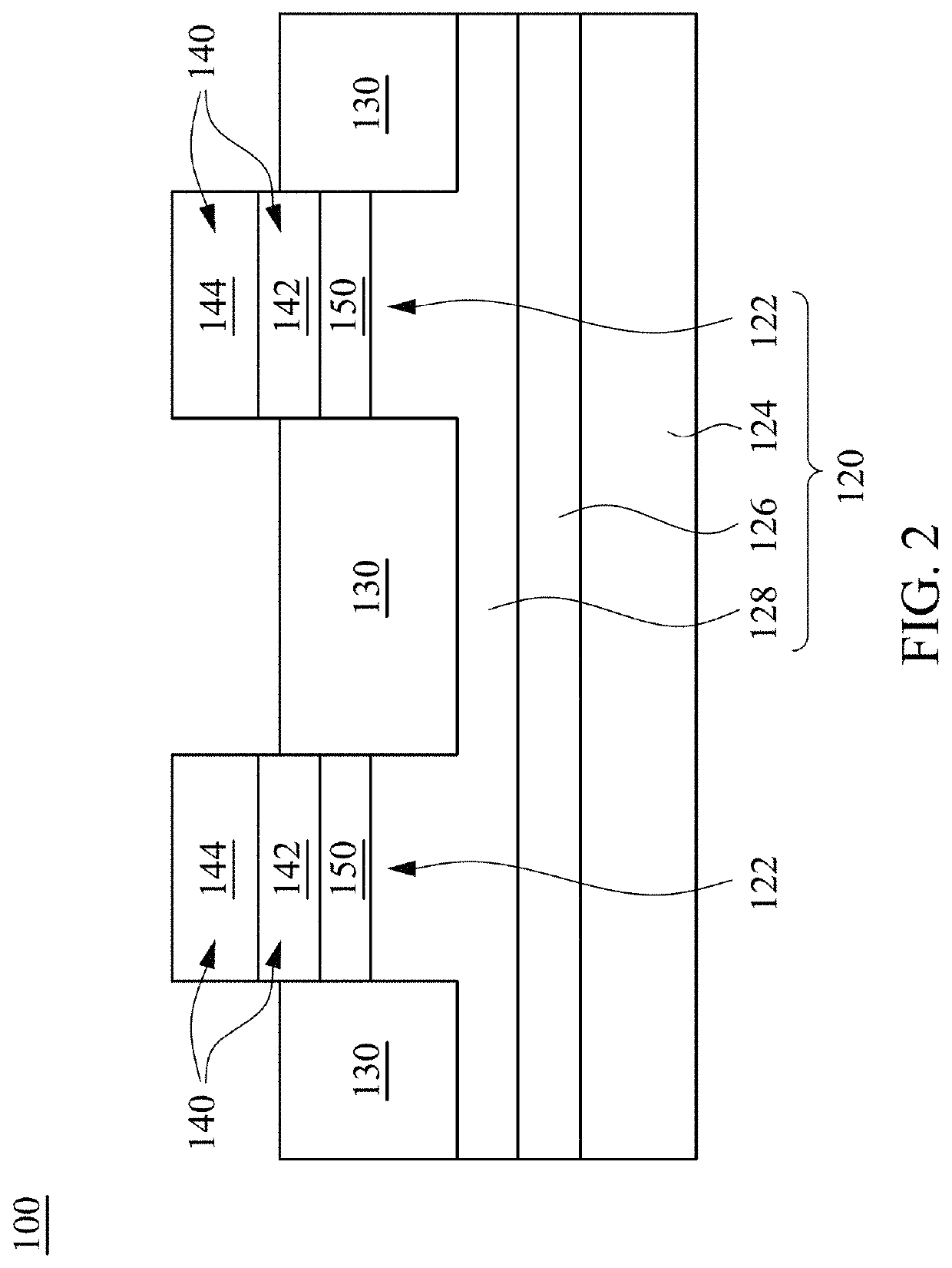
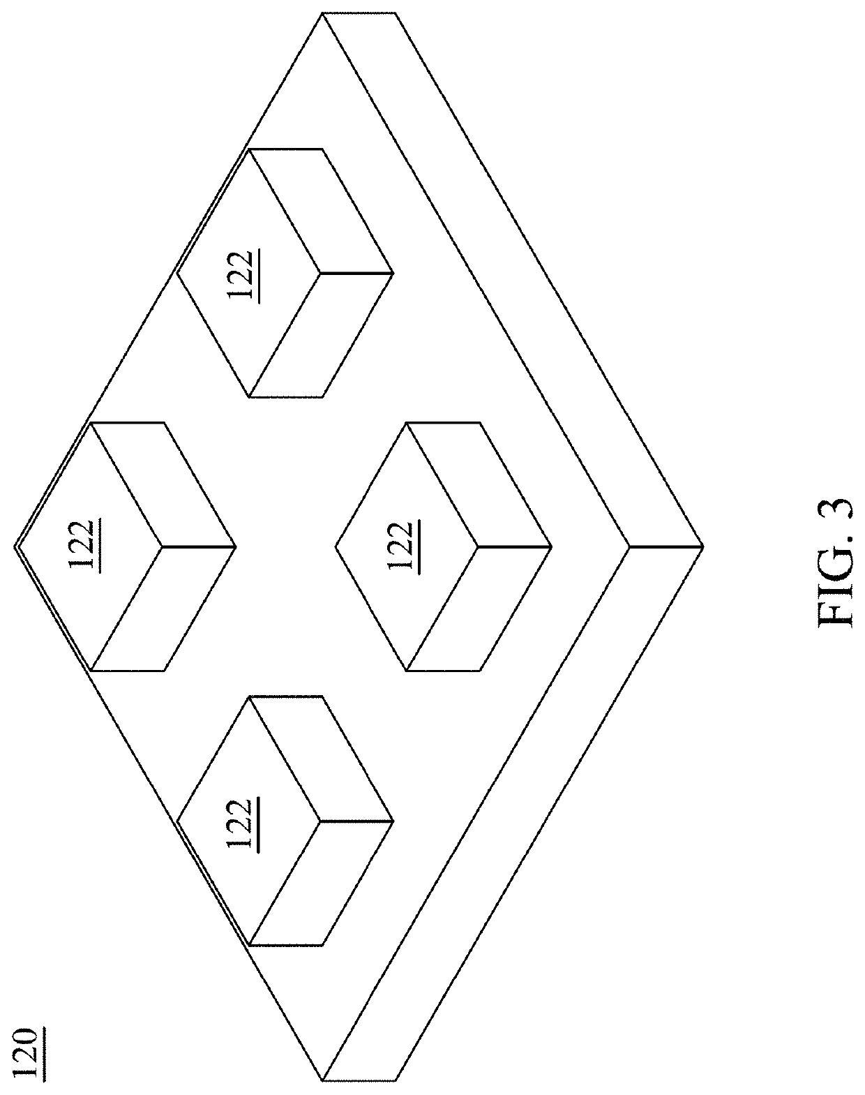
[0044]FIG. 3 illustrates a three dimensional view of the PCB 120 of the direct type backlight device 100 according to the present invention. As shown in FIGS. 1-3, the PCB 120 has plural bump structures 122. The light reflector 130 is disposed over the PCB 120 but is not disposed over the bump structures 122. The Mini-LEDs 140 is disposed over the PCB 120 and is disposed over the bump structures 122. The light reflector 130 is arranged between at least part of adjacent Mini-LEDs 140. The light reflector 130 is arranged between at least part of adjacent bump structures 122. Specifically, the light reflector 130 surrounds the Mini-LEDs 140. It is noted that the number of the Mini-LEDs 140 or the number of the bump structures 122 as shown in FIGS. 1-3 is only an example and is not intended to limit the present invention.
[0045]Each of the Mini-LEDs 140 includes a non-light-emitting layer 142 and a light-emitting layer 144 arranged on the non-light-emitting layer 142. Specifically, the n...
third embodiment
[0069]FIG. 10 illustrates a diagram showing the design change of the bonding pad 150 according to the present invention. The design change as shown in FIG. 10 could improve the self-alignment capability between the contact pads 146 and the bonding pads 150 during the reflow process, such that, when the mounting skewing is occurred, the misalignment problem could be improved. As shown in FIG. 10, each of the Mini-LEDs 140 has two contact pads 146 (i.e., one positive polarity contact pad and one negative polarity contact pad), and each of the contact pads 146 of the Mini-LED 140 would be electrically connected to two bonding pads 150 on the PCB 120. In other words, each of the contact pads 146 is electrically connected to two bonding pads 150 in a one-by-two manner.
[0070]The upper left diagram of FIG. 10 is a top view of the Mini-LED 140 and the bump structure 122 of the PCB 120. The upper right diagram of FIG. 10 is a right side view of the Mini-LED 140 and the bump structure 122 of ...
fourth embodiment
[0072]FIG. 11 illustrates a diagram showing the design change of the bonding pad 150 and the contact pad 146 according to the present invention. The design change as shown in FIG. 11 could improve the self-alignment capability between the contact pads 146 and the bonding pads 150 during the reflow process, such that, when the mounting skewing is occurred, the misalignment problem could be improved. As shown in the upper left diagram of FIG. 11, each of the Mini-LEDs 140 has four contact pads 146 (i.e., two positive polarity contact pads and two negative polarity contact pads). As shown in the bottom left diagram of FIG. 11, there are four bonding pads 150 on the bump structure 122 corresponding to each of the Mini-LEDs 140. In other embodiments of the present invention, four sub-bump structures are correspondingly formed on the PCB in the vertical projection of the said four bonding pads.
[0073]As shown in the right diagram of the FIG. 11, the said four contact pads 146 of each of th...
PUM
| Property | Measurement | Unit |
|---|---|---|
| thickness | aaaaa | aaaaa |
| distance | aaaaa | aaaaa |
| brightness | aaaaa | aaaaa |
Abstract
Description
Claims
Application Information