
Method of measuring critical dimension of a three-dimensional structure and apparatus for measuring the same

a three-dimensional structure and critical dimension technology, applied in the field of electronic device fabrication technology, can solve the problems of becoming more difficult and inaccurate to estimate the parameter vector based on a conventional numerical simulator, and more likely to obtain an incorrect parameter vector

Active Publication Date: 2022-05-03
SK HYNIX INC +1
View PDF5 Cites 0 Cited by
  • Summary
  • Abstract
  • Description
  • Claims
  • Application Information

AI Technical Summary

Benefits of technology

The present patent provides methods and apparatuses for accurately and quickly calculating a critical dimension of a three-dimensional shape by accurately and quickly calculating a parameter vector that can model a measurement spectrum, and estimating the critical dimension of the three-dimensional shape. This is achieved by using matrix information on the hypothesized parameter distribution regarding the critical dimension of the three-dimensional structure. The technical effect of this patent is to offer a reliable and efficient approach for measuring the critical dimension of a three-dimensional shape, which can be utilized in various industries such as electronics manufacturing.

Problems solved by technology

However, in estimating the nonlinear parameter, an undesired result may be caused by an estimation error, so that a gradient vector estimation or a Hessian matrix estimation may be required to be performed on each candidate solution.
Therefore, such a conventional estimation method for the nonlinear parameter becomes sensitive to the characteristics of the objective function that determines the parameter vector, and it becomes more likely to obtain an incorrect parameter vector.
Moreover, as the size of the semiconductor device such as a highly integrated circuit IC is reduced to a relatively small scale (e.g., a nano scale), it may become more difficult and inaccurate to estimate the parameter vector based on a conventional numerical simulator.

Method used


Image

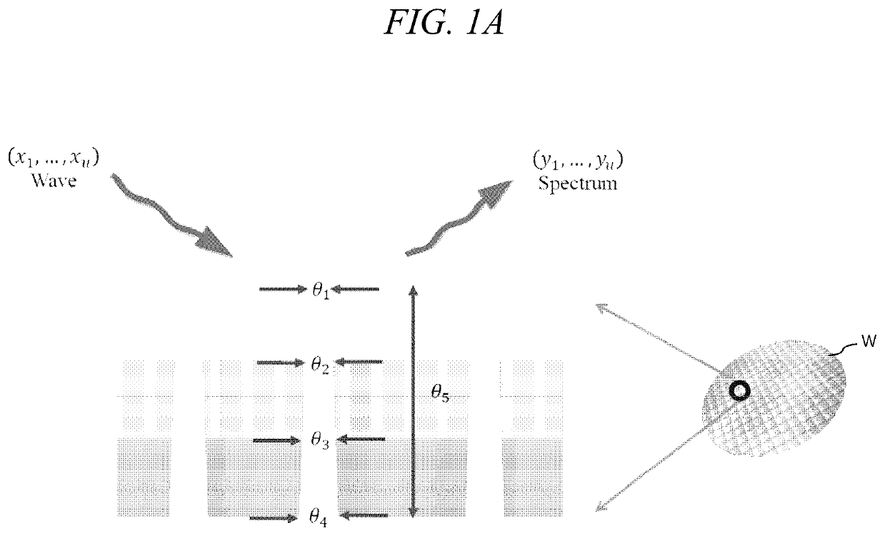
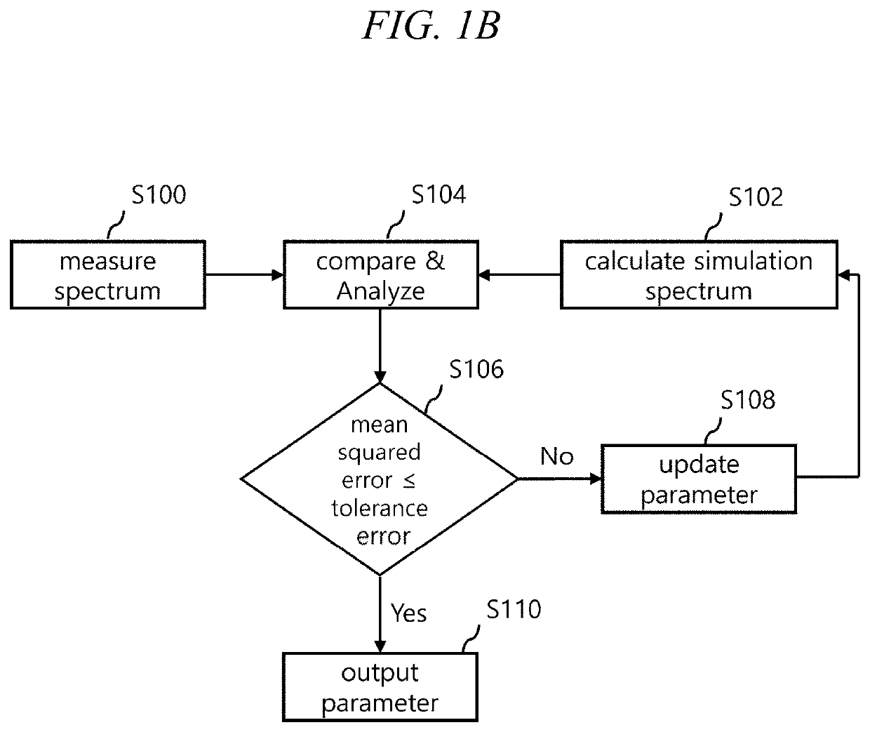
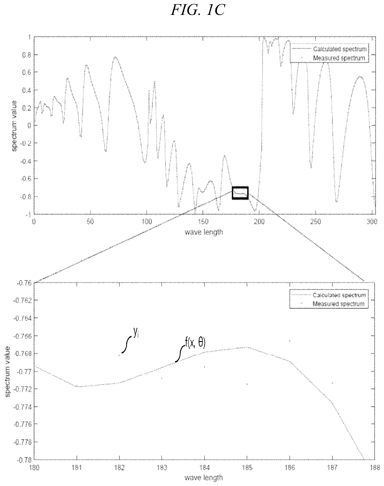
  • Method of measuring critical dimension of a three-dimensional structure and apparatus for measuring the same
  • Method of measuring critical dimension of a three-dimensional structure and apparatus for measuring the same
  • Method of measuring critical dimension of a three-dimensional structure and apparatus for measuring the same

Examples


Embodiment Construction

[0035]Hereinafter, various embodiments of the present disclosure will be described in detail with reference to the accompanying drawings.

[0036]The embodiments of the present disclosure are provided to more completely describe the present disclosure to those having a common knowledge in the related art, and the following embodiments may be modified in various other forms, and the scope of the present disclosure is not limited to the embodiments. Rather, these embodiments are provided to describe the present disclosure more faithfully and completely, and to fully convey the spirit of the present disclosure to those skilled in the art.

[0037]Further, in the following drawings, the thickness or size of each layer is exaggerated for convenience and clarity of description, and the same reference numerals in the drawings refer to the same elements. As used herein, the term, “and / or” includes any one and all combinations of one or more of the listed items.

[0038]The terminology used herein is...


PUM

PropertyMeasurementUnit
aspect ratioaaaaaaaaaa
critical dimensionaaaaaaaaaa
wavelengthaaaaaaaaaa

Abstract

A method of measuring a critical dimension comprises determining matrix information on a hypothesized parameter distribution on the critical dimension; obtaining a measurement spectrum for each wavelength of a light reflected from the three-dimensional structure; sampling a first candidate parameter vector for determining a numerical simulation spectrum that approximates the measurement spectrum; linearly transforming the first candidate parameter vector by using the matrix information; determining a first candidate parameter which minimizes a difference between the measurement spectrum and the numerical simulation spectrum within the linearly transformed first candidate parameter vector; determining a second candidate parameter vector derived from the first candidate parameter and having the hypothesized parameter distribution by using a heuristic algorithm; determining a second candidate parameter that minimizes a difference between the measurement spectrum and the numerical simulation spectrum within the second candidate parameter vector; and updating the first candidate parameter by using the second candidate parameter.

Description

CROSS-REFERENCES TO RELATED APPLICATION[0001]The present application claims the benefit of Korean patent application number 10-2020-0033894, filed on Mar. 19, 2020, which is herein incorporated by reference in its entirety.BACKGROUND OF THE DISCLOSURE1. Field[0002]The present disclosure relates to an electronic device fabrication technology, and more particularly, to a method of measuring a critical dimension of a three-dimensional structure constituting a device and apparatus for measuring the same.2. Description of the Related Art[0003]In the process of fabricating an electronic device, for example, a semiconductor device such as a transistor, a memory device, or a processor, a critical dimension (CD) of three-dimensional shape (or a three-dimensional structure) of the electronic device may be measured in order to confirm the geometric size of the three-dimensional shape that affects the electrical or physical performance of the semiconductor device, for example, a line width, a t...

Claims


Application Information

Patent Timeline
Patent Type & Authority Patents(United States)
IPC IPC(8): G03F1/36G03F7/20G06F30/398
CPCG03F1/36G03F7/70625G03F7/70683G06F30/398G03F7/70616G01B9/02007G06F17/16
Inventor PARK, CHULJINKIM, HYUNGJIN
Owner SK HYNIX INC
Learn More