
Photoelectric conversion element and solid-state imaging apparatus

Active Publication Date: 2022-05-03
SONY SEMICON SOLUTIONS CORP
View PDF10 Cites 1 Cited by
  • Summary
  • Abstract
  • Description
  • Claims
  • Application Information

AI Technical Summary

Benefits of technology

The patent text describes a new way to make a photoelectric conversion element and a solid-state imaging apparatus that are more reliable. This is done by using materials with different average particle diameters. This results in a more dense organic photoelectric conversion layer with fewer voids. This improves the reliability of the apparatus and helps to capture high-quality images without any issues.

Problems solved by technology

Incidentally, in an organic photoelectric conversion element including an organic photoelectric conversion layer in which a plurality of kinds of organic semiconductor materials is mixed, occurrence of a device failure resulting from a short circuit or the like between a pair of electrodes opposed to each other with the organic photoelectric conversion layer interposed therebetween has become an issue, and an improvement in reliability is desired.

Method used


Image

  • Photoelectric conversion element and solid-state imaging apparatus
  • Photoelectric conversion element and solid-state imaging apparatus
  • Photoelectric conversion element and solid-state imaging apparatus

Examples


application examples

3. Application Examples

4. Examples

1. Embodiment

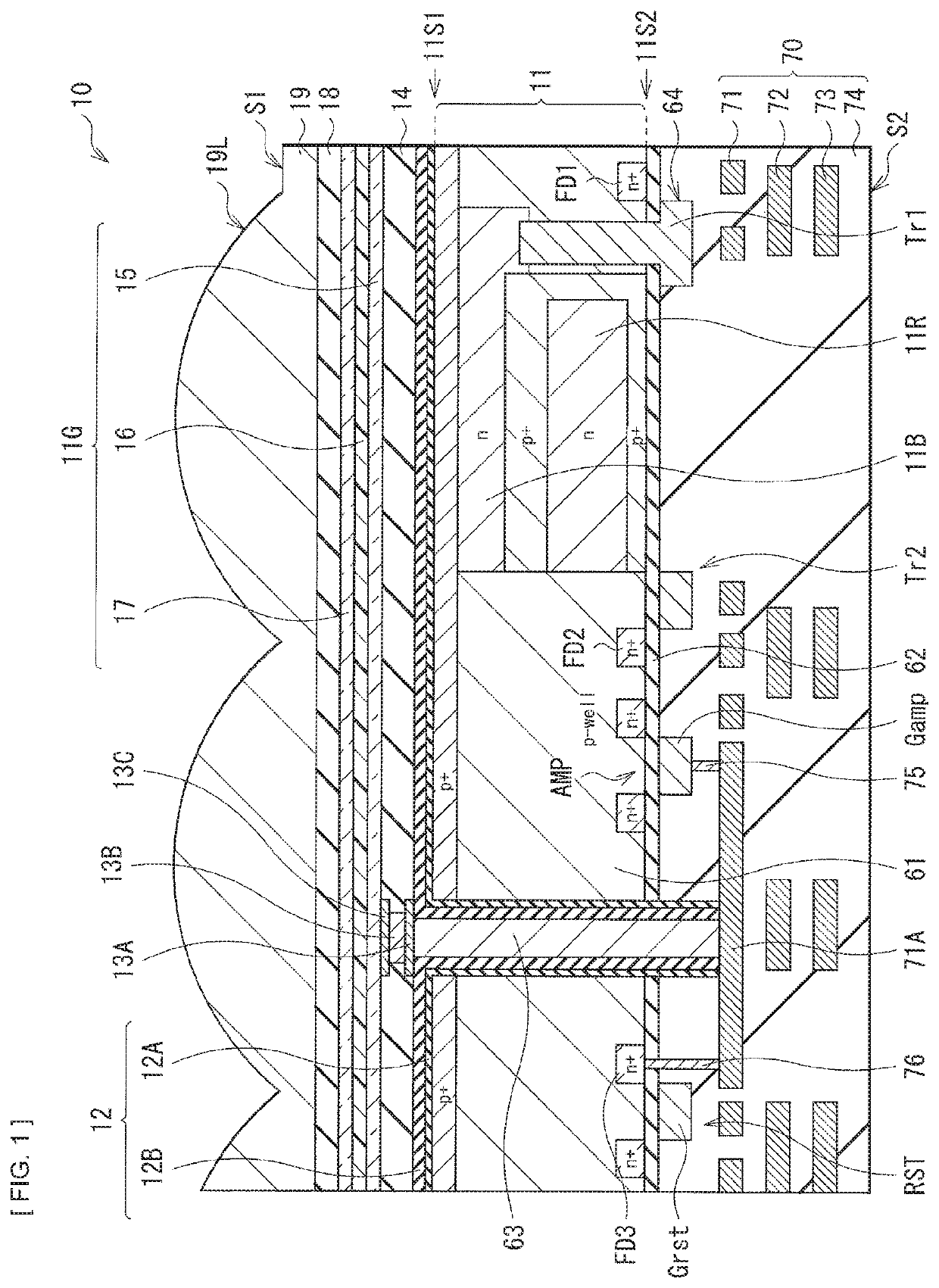
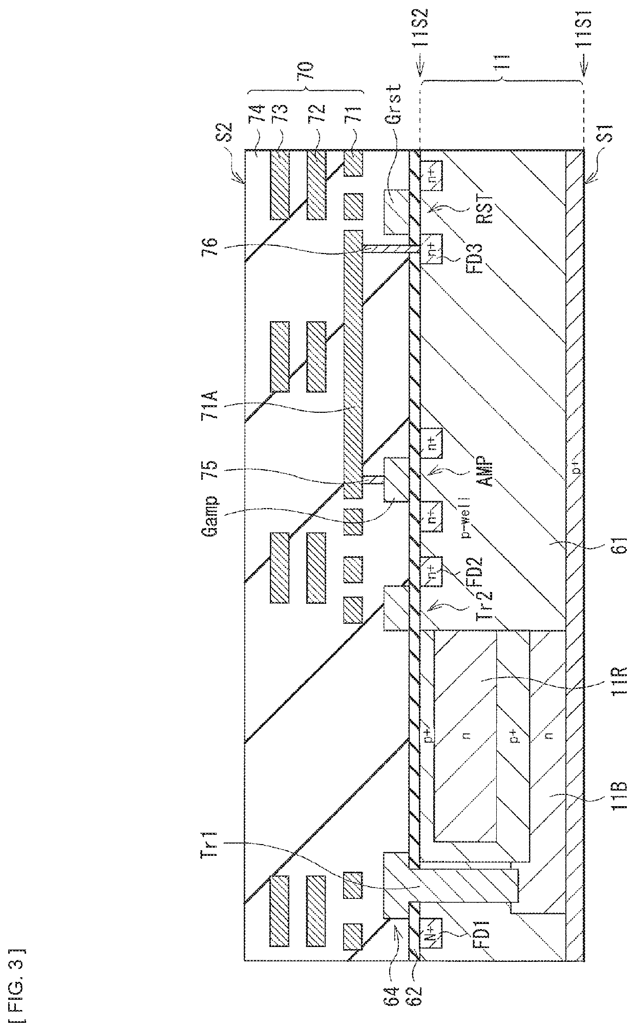
[0031]FIG. 1 illustrates a cross-sectional configuration of a photoelectric conversion element (photoelectric conversion element 10) according to an embodiment of the present disclosure. The photoelectric conversion element 10 is included in one pixel (unit pixel P) of a solid-state imaging apparatus (solid-state imaging apparatus 1) such as a back-side illumination type (back-side light reception type) CCD (Charge Coupled Device) image sensor or a CMOS (Complementary Metal Oxide Semiconductor) image sensor (refer to FIG. 7). The photoelectric conversion element 10 is of a so-called longitudinal spectral type in which one organic photoelectric converter 11G and two inorganic photoelectric converters 11B and 11R are stacked in a longitudinal direction. In the present embodiment, an organic photoelectric conversion layer 16 included in the organic photoelectric converter 11G has a configuration formed using a plurality of materials having...

modification examples

2. Modification Examples

[0107]FIG. 6 illustrates a cross-sectional configuration of a photoelectric conversion element (photoelectric conversion element 20) according to a modification example of the present disclosure. The photoelectric conversion element 20 is an imaging element included in one unit pixel P of a solid-state imaging element (solid-state imaging apparatus 1) such as a back-side illumination type CCD image sensor or a CMOS image sensor, as with the photoelectric conversion element 10 according to the above-described embodiment and the like. The photoelectric conversion element 20 according to the present modification example has a configuration in which a red photoelectric converter 40R, a green photoelectric converter 40G, and a blue photoelectric converter 40B are stacked in this order on a silicon substrate 81 with an insulating layer 82 interposed therebetween.

[0108]The red photoelectric converter 40R, the green photoelectric converter 40G, and the blue photoelec...

application example

3. Application Example

Application Example 1

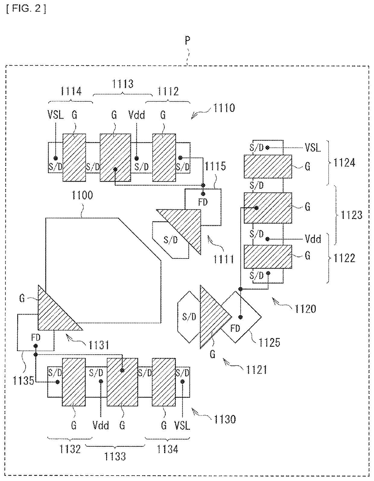
[0128]FIG. 7 illustrates an overall configuration of the solid-state imaging apparatus 1 using, for each of the pixels, the photoelectric conversion element 10 described in the above-described embodiment. The solid-state imaging apparatus 1 is a CMOS image sensor, and includes, on the semiconductor substrate 11, a pixel section 1a as an imaging region and a peripheral circuit section 130 including, for example, a row scanner 131, a horizontal selector 133, a column scanner 134, and a system controller 132 in a peripheral region of the pixel section 1a.

[0129]The pixel section 1a has a plurality of unit pixels P (each corresponding to the photoelectric conversion element 10) two-dimensionally arranged in a matrix, for example. The unit pixels P are wired with pixel drive lines Lread (specifically, row selection lines and reset control lines) for respective pixel rows, and vertical signal lines Lsig for respective pixel columns, for example. ...


PUM

PropertyMeasurementUnit
surface roughness Raaaaaaaaaaa
particle diameteraaaaaaaaaa
wavelength bandaaaaaaaaaa

Abstract

A photoelectric conversion element according to an embodiment of the present disclosure includes: a first electrode; a second electrode opposed to the first electrode; and an organic photoelectric conversion layer provided between the first electrode and the second electrode and formed using a plurality of materials having average particle diameters different from each other, the plurality of materials including at least fullerene or a derivative thereof.

Description

CROSS REFERENCE TO RELATED APPLICATIONS[0001]This application is a U.S. National Phase of International Patent Application No. PCT / JP2018 / 040215 filed on Oct. 30, 2018, which claims priority benefit of Japanese Patent Application No. JP 2017-221739 filed in the Japan Patent Office on Nov. 17, 2017. Each of the above-referenced applications is hereby incorporated herein by reference in its entirety.TECHNICAL FIELD[0002]The present disclosure relates to a photoelectric conversion element using an organic semiconductor material and a solid-state imaging apparatus including the same.BACKGROUND ART[0003]In recent years, devices using organic thin films have been developed. An organic photoelectric conversion element is one of the devices, and an organic thin-film solar cell, an organic imaging element, and the like each using the organic photoelectric conversion element have been proposed. The organic photoelectric conversion element adopts a bulk heterostructure in which a p-type organi...

Claims


Application Information

Patent Timeline
Patent Type & Authority Patents(United States)
IPC IPC(8): H01L51/42H01L27/28H01L51/44H01L27/30H01L27/146
CPCH01L51/4253H01L27/286H01L27/307H01L51/442H01L27/14647H01L31/10Y02E10/549H01L27/14667H01L27/1464H01L27/14601H10K39/00H10K39/32H10K85/211H10K30/30H10K19/20H10K30/82
Inventor TAKAHASHI, SHINGO
Owner SONY SEMICON SOLUTIONS CORP
Learn More