Method for performing access management of memory device with aid of information arrangement, associated memory device and controller thereof, associated electronic device

a memory device and information arrangement technology, applied in the direction of memory address/allocation/relocation, fault response, instruments, etc., can solve the problems of inability to work for memory devices equipped with quadruple level cell (qlc) flash memory, instability of mlc flash memory, increased bit error rate, etc., to improve read performance of memory controller, increase bit error rate, and degrade system reliability

Active Publication Date: 2022-06-07
SILICON MOTION INC (TW)
View PDF10 Cites 0 Cited by
  • Summary
  • Abstract
  • Description
  • Claims
  • Application Information

AI Technical Summary

Benefits of technology

[0011]In addition to the above method, the present invention also provides a controller of a memory device, where the memory device comprises the controller and a NV memory. The NV memory may comprise at least one NV memory element (e.g. one or more NV memory elements). In addition, the controller comprises a processing circuit that is arranged to control the controller according to a plurality of host commands from a host device, to allow the host device to access the NV memory through the controller. For example, if the host device sends a write command to the memory device, the controller generates a plurality of ECC chunks respectively corresponding to a plurality of sets of memory cells of the NV memory according to data, for establishing one-to-one mapping between the plurality of ECC chunks and the plurality of sets of memory cells, wherein the plurality of host commands comprises the write command. Additionally, the controller stores the plurality of ECC chunks into the plurality of sets of memory cells, respectively, to prevent any two ECC chunks of the plurality of ECC chunks from sharing a same set of memory cells of the plurality of sets of memory cells, to enhance read performance of the memory controller regarding the data.
[0012]The present invention method and associated apparatus can guarantee that the whole system (e.g. the host device and the memory device) can operate properly, to prevent problems in the related art, such as the increased bit error rate, degraded system reliability due to the weakest page, etc. In addition, implementing the embodiments of the present invention does not significantly increase additional costs. Therefore, the related art problems can be solved, and the overall cost will not increase too much. In comparison with the related art, the present invention method and associated apparatus can enhance overall performance without introducing any side effect or in a way that is less likely to introduce a side effect.

Problems solved by technology

Improving access control of memories in these memory devices remains an issue to be solved in the art.
The MLC flash memory does have instability issues, however.
For example, as the triple level cell (TLC) flash memories have been applied to the memory devices, there are some problems such as an increased bit error rate, etc.
Although a traditional sensing scheme regarding reading data from the TLC flash memories has been proposed to try solving the problems, it does not work for the memory devices equipped with the quadruple level cell (QLC) flash memories.
More particularly, the traditional sensing scheme is not good for high-level per memory cell in the QLC flash memories, and system reliability will be bounded by the weakest page.

Method used


Image

  • Method for performing access management of memory device with aid of information arrangement, associated memory device and controller thereof, associated electronic device
  • Method for performing access management of memory device with aid of information arrangement, associated memory device and controller thereof, associated electronic device
  • Method for performing access management of memory device with aid of information arrangement, associated memory device and controller thereof, associated electronic device

Examples


Embodiment Construction

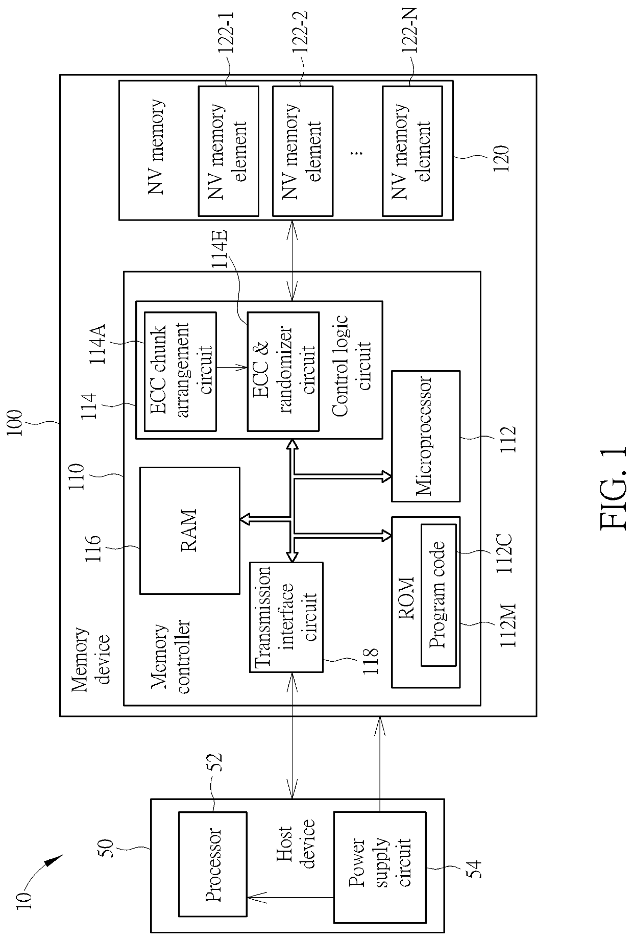
[0025]FIG. 1 is a diagram of an electronic device 10 according to an embodiment of the present invention, where the electronic device 10 may comprise a host device 50 and a memory device 100. The host device 50 may comprise at least one processor (e.g. one or more processors) which may be collectively referred to as the processor 52, and may further comprise a power supply circuit 54 coupled to the processor 52. The processor 52 is arranged for controlling operations of the host device 50, and the power supply circuit 54 is arranged for providing power to the processor 52 and the memory device 100, and outputting one or more driving voltages to the memory device 100. The memory device 100 may be arranged for providing the host device 50 with storage space, and obtaining the one or more driving voltages from the host device 50 as power source of the memory device 100. Examples of the host device 50 may include, but are not limited to: a multifunctional mobile phone, a wearable device...


PUM


Abstract

A method for performing access management of a memory device with aid of information arrangement and associated apparatus (e.g. the memory device and controller thereof, and an associated electronic device) are provided. The method may include: when the host device sends a write command to the memory device, utilizing the memory controller to generate a plurality of ECC chunks respectively corresponding to a plurality of sets of memory cells of the NV memory according to data, for establishing one-to-one mapping between the plurality of ECC chunks and the plurality of sets of memory cells; and utilizing the memory controller to store the plurality of ECC chunks into the plurality of sets of memory cells, respectively, to prevent any two ECC chunks of the ECC chunks from sharing a same set of memory cells of the sets of memory cells, to enhance read performance of the memory controller regarding the data.

Description

BACKGROUND OF THE INVENTION1. Field of the Invention[0001]The present invention relates to access control of flash memory, and more particularly, to a method for performing access management of a memory device with aid of information arrangement, and associated apparatus (e.g. the memory device and controller thereof such as a memory controller within the memory device, and an associated electronic device).2. Description of the Prior Art[0002]Developments in memory technology have led to the wide application of portable or non-portable memory devices, such as memory cards which conform to the SD / MMC, CF, MS and XD specifications, respectively, solid state drives (SSDs), or embedded memory devices which conform to the UFS and eMMC specifications, respectively. Improving access control of memories in these memory devices remains an issue to be solved in the art.[0003]NAND flash memories may comprise single level cell (SLC) and multiple level cell (MLC) flash memories. In an SLC flash ...

Claims


Application Information

Patent Timeline
Patent Type & Authority Patents(United States)
IPC IPC(8): G06F12/02G11C11/56G06F3/06G06F11/10
CPCG06F12/0246G06F3/064G06F3/0658G06F3/0659G06F3/0679G06F11/1072G11C11/5628G11C11/5642G06F3/0614G06F11/1068G06F11/108G11C16/0483G06F3/061G06F3/0688G06F2212/7201G06F2212/7209G06F11/1048
Inventor YANG, TSUNG-CHIEH
Owner SILICON MOTION INC (TW)
Why Eureka
Try Eureka