
Organic light emitting diode display panel having groove structure in thin film packaging layer to improve adhesion and method of manufacturing thereof

a technology of organic light-emitting diodes and thin film packaging layers, which is applied in the field of display, can solve the problems of easy misalignment or peeling, affecting the quality of the inner film layer, and affecting the quality of the display panel, and urgent improvement is needed

Active Publication Date: 2022-08-02
WUHAN CHINA STAR OPTOELECTRONICS SEMICON DISPLAY TECH CO LTD
View PDF13 Cites 0 Cited by
  • Summary
  • Abstract
  • Description
  • Claims
  • Application Information

AI Technical Summary

Benefits of technology

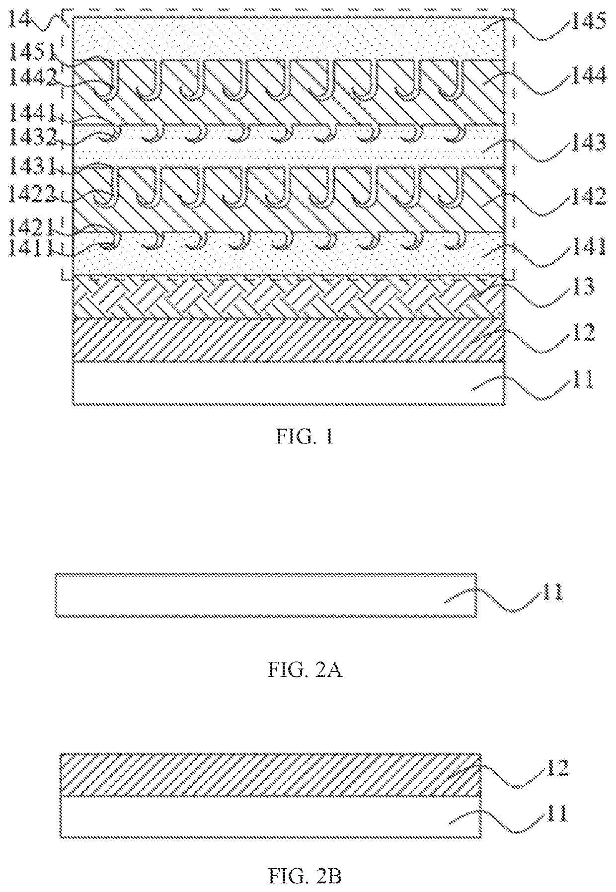
The present invention provides an OLED display panel that has better adhesion and stability compared to prior art. A groove structure in the thin film packaging layer improves the stability of the display panel when subjected to bending or lateral pressure. The groove is divided into two parts to further improve stability. The packaging layer has a multi-layer structure that reduces the risk of peeling. These technical effects contribute to improved quality and performance of the OLED display panel.

Problems solved by technology

However, in a conventional thin film package, due to interface of the organic layer and the inorganic layer are generally flat and smooth, and due to the organic layer and the inorganic layer are different in material, when the bending or lateral stress is applied, it is easy to be misaligned or peeled off, so that external water, oxygen, impurities, and the like invade the inner film layer may affect the quality of the inner film layer.
Therefore, in the conventional OLED display technology, stability and adhesion between the inorganic layer and the organic layer of the thin film packaging structure are poor, so that the inner film layer is easily affected by external water, oxygen, and impurities, and thus the problems of affecting the quality of the display panel are in urgent need of improvement.

Method used


Image

  • Organic light emitting diode display panel having groove structure in thin film packaging layer to improve adhesion and method of manufacturing thereof
  • Organic light emitting diode display panel having groove structure in thin film packaging layer to improve adhesion and method of manufacturing thereof
  • Organic light emitting diode display panel having groove structure in thin film packaging layer to improve adhesion and method of manufacturing thereof

Examples


Embodiment Construction

[0048]The preferred embodiments of the present invention are described in detail below with reference to the accompanying drawings. Those skilled persons in the art will easily understand how to implement the invention. The invention can be implemented by the embodiments, so that the technical content of the disclosure will be clear, so that those skilled persons in the art will understand how to implement the invention. The present invention may be accomplished in many different embodiments, and the scope of the invention is not limited to the embodiments described herein.

[0049]In the description of the present invention, it should be understood that the terms “center,”“longitudinal,”“transverse,”“length,”“width,”“thickness,”“upper,”“lower,”“front,”“back,”“left,”“right,”“vertical,”“horizontal,”“top,”“bottom,”“inside,”“outside,”“clockwise,”“counterclockwise,” etc. The positional relationship is based on the orientation or positional relationship shown in the drawings, and is merely ...


PUM

PropertyMeasurementUnit
lengthaaaaaaaaaa
lengthaaaaaaaaaa
depthaaaaaaaaaa

Abstract

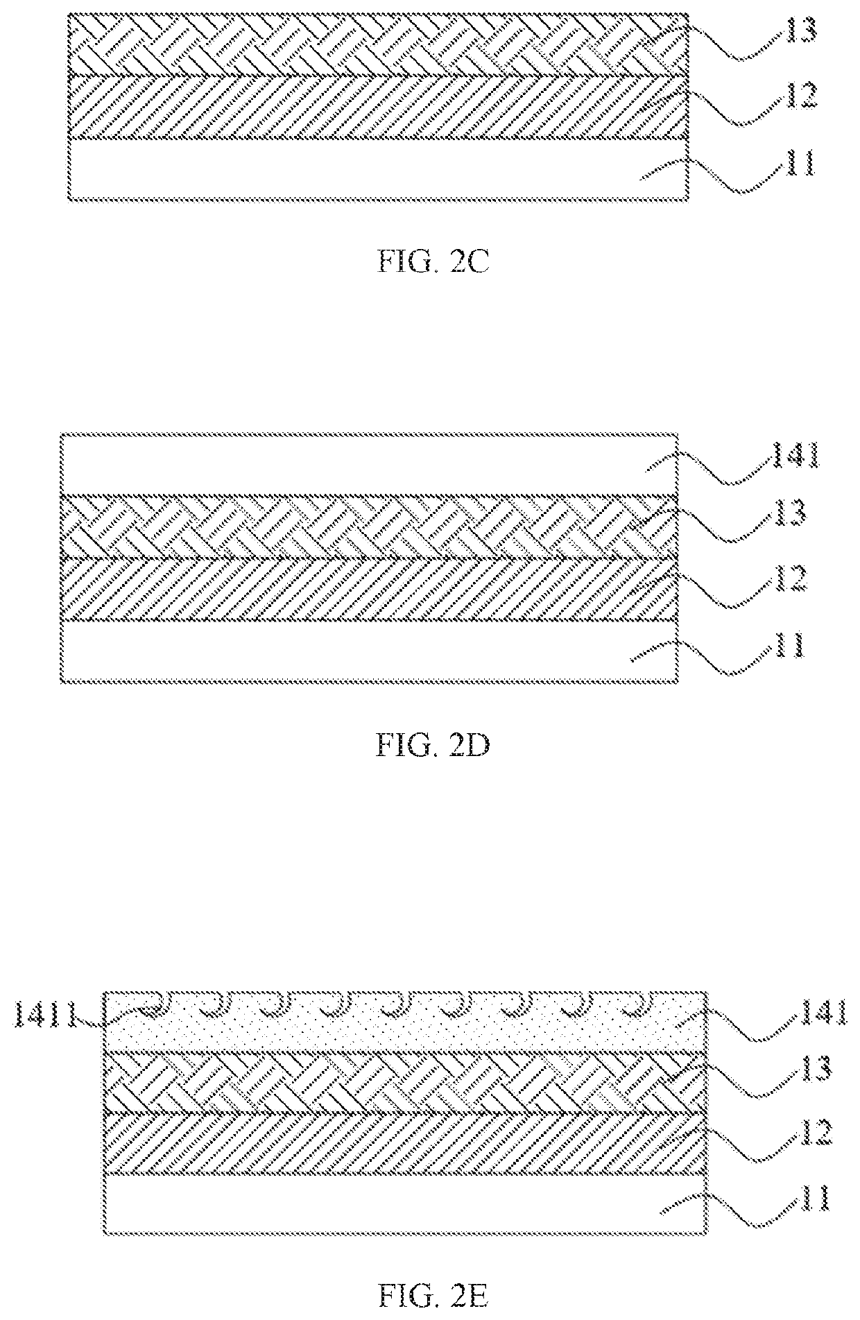
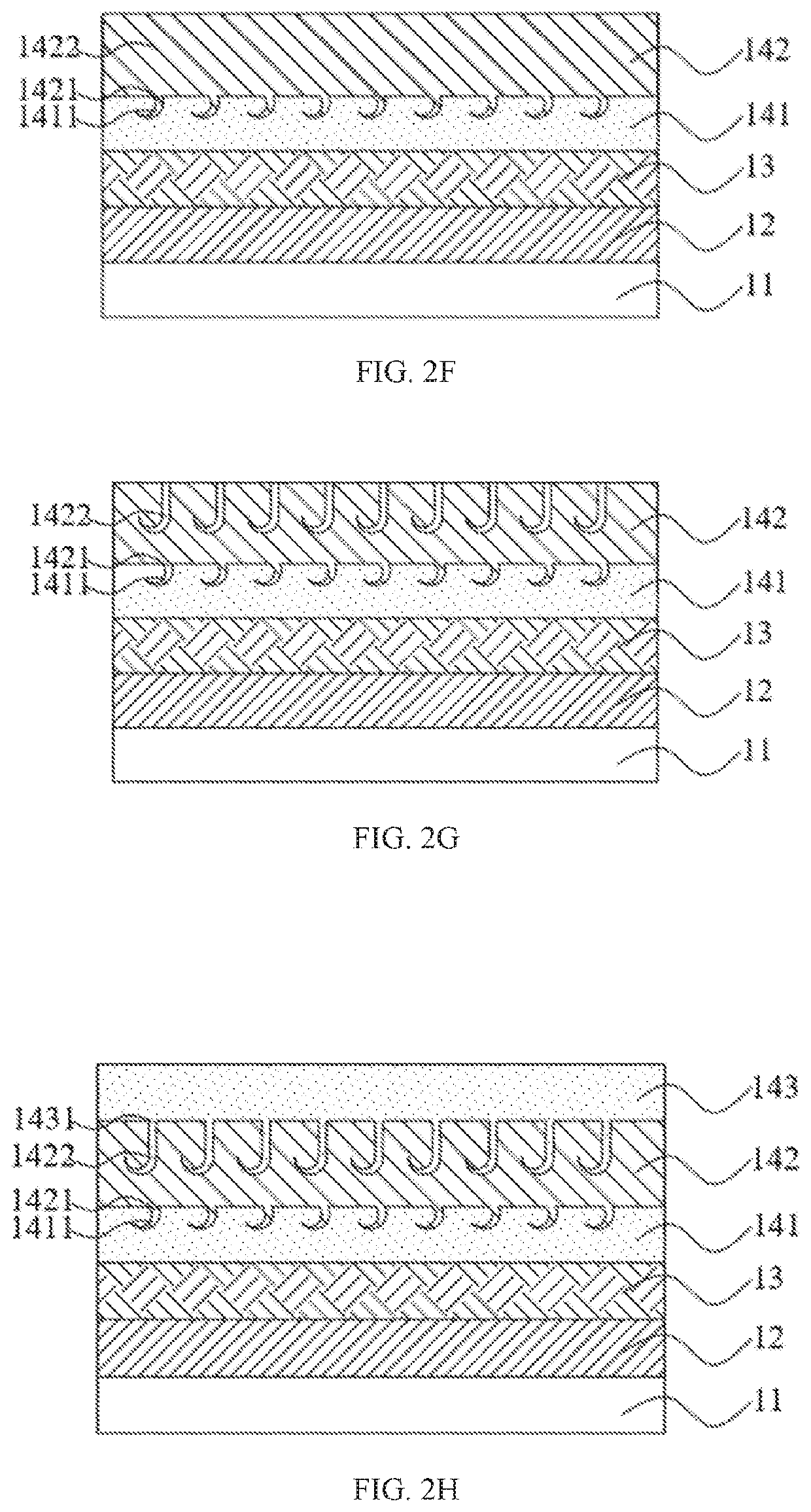
An organic light emitting diode (OLED) display panel and a method of manufacturing the same are provided. The OLED display panel includes a base substrate, a thin film transistor layer, an OLED device layer and a packaging layer sequentially disposed. The packaging layer includes a first inorganic packaging layer, a first organic layer and a second inorganic packaging layer sequentially disposed. The first inorganic packaging layer is formed with a first groove and the first organic packaging layer is formed with a second groove.

Description

CROSS-REFERENCE TO RELATED APPLICATIONS[0001]This application is a U.S. National Phase of International PCT Application No. PCT / CN2019 / 111861 filed Oct. 18, 2019, which claims the benefit of Chinese Patent Application Serial No. 201910765657.X filed Aug. 19, 2019, the contents of each application are incorporated herein by reference in their entirety.BACKGROUND OF INVENTIONField of Invention[0002]The present invention relates to the field of display, and more particularly, to an organic light emitting diode (OLED) display panel and a method of manufacturing the same.Description of Prior Art[0003]Recently, organic light emitting diode (OLED) display technology has developed by leaps and bounds. OLED products have attracted more and more attention and applications due to their advantages of lightness, fast responses, wide viewing angles, high contrast and flexibility, and mainly used in display fields such as mobile phones, tablets and televisions.[0004]An OLED display panel includes ...

Claims


Application Information

Patent Timeline
Patent Type & Authority Patents(United States)
IPC IPC(8): H01L51/52H01L27/32H01L51/56
CPCH01L51/5253H01L27/3244H01L51/56H01L2227/323H10K59/1201H10K59/8731H10K50/844H10K59/12H10K71/00
Inventor LI, ZHAO
Owner WUHAN CHINA STAR OPTOELECTRONICS SEMICON DISPLAY TECH CO LTD
Learn More