Manufacturing method for a semiconductor device

a manufacturing method and technology of semiconductor devices, applied in the direction of semiconductor devices, basic electric elements, electrical appliances, etc., can solve the problems of unrepaired lattice damage, unrepaired lattice damage, and complex structure of memory transistor sources

Active Publication Date: 2022-10-04
SHANGHAI HUALI MICROELECTRONICS CORP
View PDF2 Cites 0 Cited by
  • Summary
  • Abstract
  • Description
  • Claims
  • Application Information

AI Technical Summary

Benefits of technology

[0029]According to the manufacturing method for the semiconductor device provided in the present invention, the step of lightly doped drain ion implantation in the memory area is executed, and on the premise that we don't change the structure and the design of the original device and adjusting the ion implantation conditions, the physical structure before implantation is simpler, the possibility that implanted ions are blocked by defects is reduced, and in addition, damage caused by ion implantation is repaired by means of increased thermal budget from the subsequent process, and at the same time the ion diffusion is more uniform. Finally, the effect of improving the electrical uniformity of the memory cell is achieved, and the yield and the erase performance of the flash memory cell are effectively improved. Moreover, according to the manufacturing method for the semiconductor device provided in the present invention, when lightly doped drain ion implantation is performed on the memory area, no need to add the photo resist in the peripheral device area, such that we can save a layer of photomask, thus the manufacturing cost may be reduced.

Problems solved by technology

1. After self-aligned source etching, the structure of the memory transistor source is complicated, so it is easy to include defects such as particles in the trench, and these defects may block some of the cell LDD implantation; and
2. The thermal budget may not be sufficient after cell LDD implantation, leading to unrepaired lattice damage caused by ion implantation and non-uniform ion diffusion.
The above two aspects may result in poor device uniformity among memory transistors.
When an erase function of all memory cells on the same chip does not occur in the same interval, a serious condition such as an erase failure may result in poor device performance.

Method used


Image

  • Manufacturing method for a semiconductor device
  • Manufacturing method for a semiconductor device
  • Manufacturing method for a semiconductor device

Examples


Embodiment Construction

[0037]The present invention will be described in detail in conjunction with the accompanying drawings and the specific embodiments. It should be noted that the aspects described below in conjunction with the accompanying drawings and the specific embodiments are merely exemplary and should not be construed as limiting the scope of protection of the present invention.

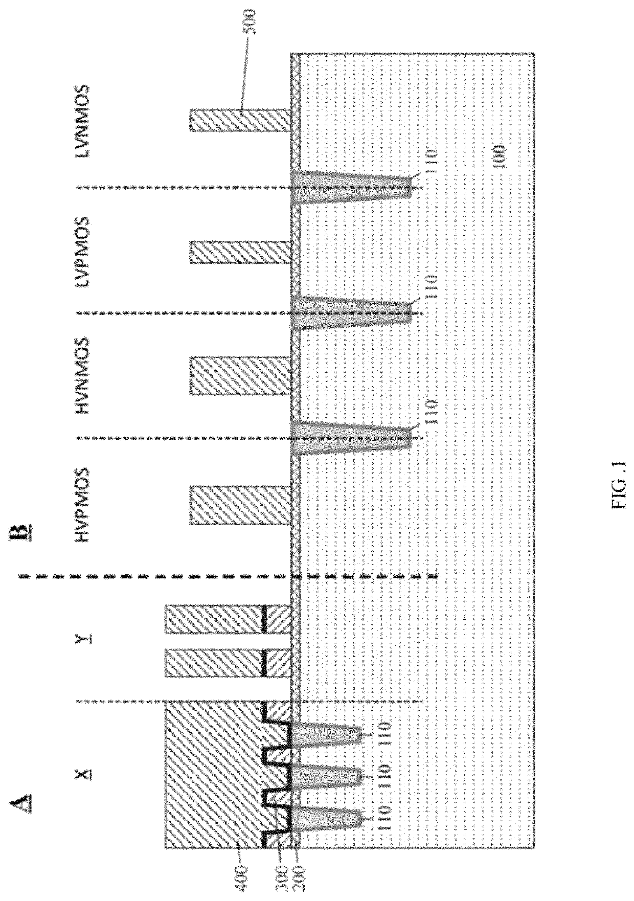
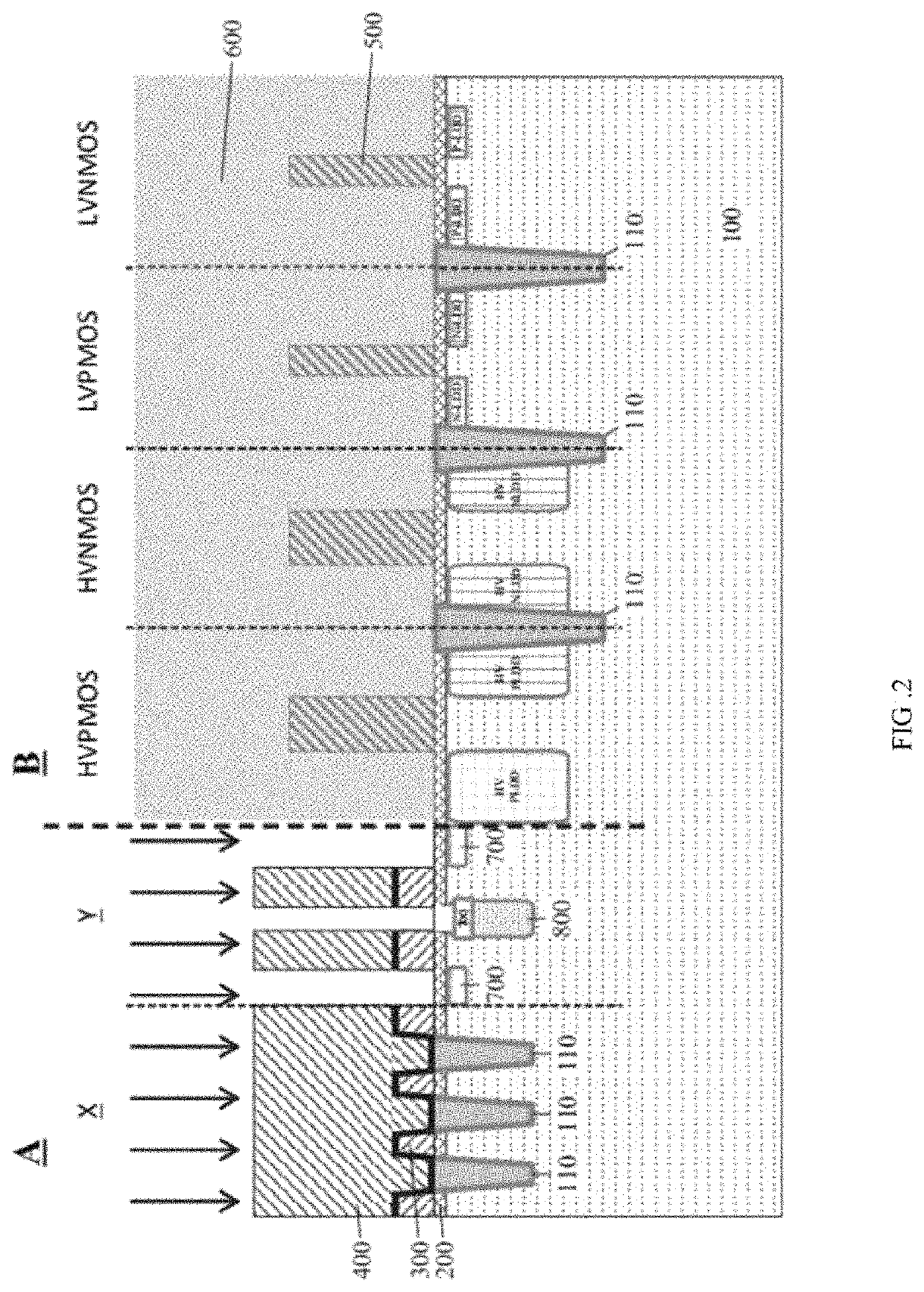
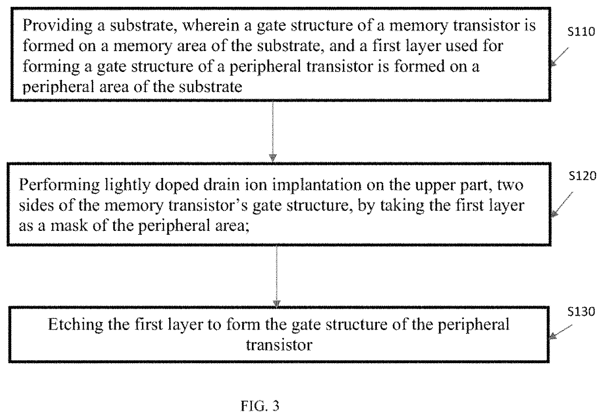
[0038]The present invention relates to a manufacturing method for a semiconductor device. According to one embodiment of the present disclosure, to avoid the two weaknesses of an existing cell LDD implantation process, by carrying out the step of light doped drain ion implantation in the storage area in advance, on the premise without changing the structure and the design of an original device and keeping the ion implantation conditions, the physical structure before implantation is simpler, thus the possibility to have implanted ions blocked by defects is reduced, in addition, damage caused by ion implantation is also r...


PUM

PropertyMeasurementUnit
areaaaaaaaaaaa
non-volatilityaaaaaaaaaa
memory areaaaaaaaaaaa

Abstract

The present invention provides a manufacturing method for a semiconductor memory device. The method comprises: providing a substrate, wherein a gate structure of a memory transistor is formed on a memory area of the substrate, and a first layer used for forming a gate structure of a peripheral transistor is formed on a peripheral area of the substrate; performing lightly doped drain ion implantation on an upper part of a portion, on two sides of the gate structure of the memory transistor, of the memory area of the substrate by applying the first layer as a mask of the peripheral area; and etching the first layer to form the gate structure of the peripheral transistor. According to the present invention, an ion diffusion degree of source and drain electrodes of the memory area may be effectively increased, and the uniformity of a memory cell device is improved.

Description

CROSS-REFERENCES TO RELATED APPLICATIONS[0001]This application claims priority to Chinese patent application No. CN202010489472.3 filed on Jun. 2, 2020, and entitled “MANUFACTURING METHOD FOR A SEMICONDUCTOR DEVICE”, the disclosure of which is incorporated herein by reference in entirety.TECHNICAL FIELD[0002]The present invention relates to semiconductor device manufacturing technology, in particular, to a manufacturing method for a flash memory.BACKGROUND[0003]Flash memory devices have the advantages of non-volatility, easy programming and erasing, long service life, and low cost, etc. and have been widely applied to various fields including consumer electronics, network communication apparatuses, industrial instrument and meter embedded systems, automobile devices, etc.[0004]In existing flash memory device structures, a NOR flash structure, for example, has three different gates:[0005]1. a floating gate (also abbreviated as FG) of a memory transistor in a memory area, which is a b...

Claims


Application Information

Patent Timeline
Patent Type & Authority Patents(United States)
IPC IPC(8): H01L29/66
CPCH01L29/66492H01L29/66825H10B41/00H10B41/42H10B41/60H10B41/30H01L29/66575H10B41/49
Inventor PENG, XIANGCHEN, HAOYUWANG, QIWEI
Owner SHANGHAI HUALI MICROELECTRONICS CORP
Why Eureka
Try Eureka