

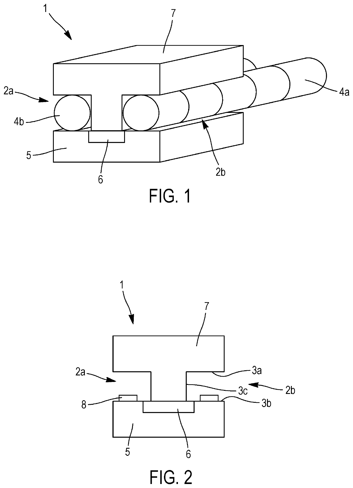
Radiofrequency transmission/reception device
a technology of radiofrequency and transmission device, which is applied in the direction of loop antennas with ferromagnetic cores, resonant antennas, instruments, etc., can solve the problems of relatively cumbersome transmission-reception devices formed from these chips, and cannot be integrated into all kinds of objects, so as to achieve favorable form factors
- Summary
- Abstract
- Description
- Claims
- Application Information
AI Technical Summary
Benefits of technology
Problems solved by technology
Method used
Image

Examples
first embodiment
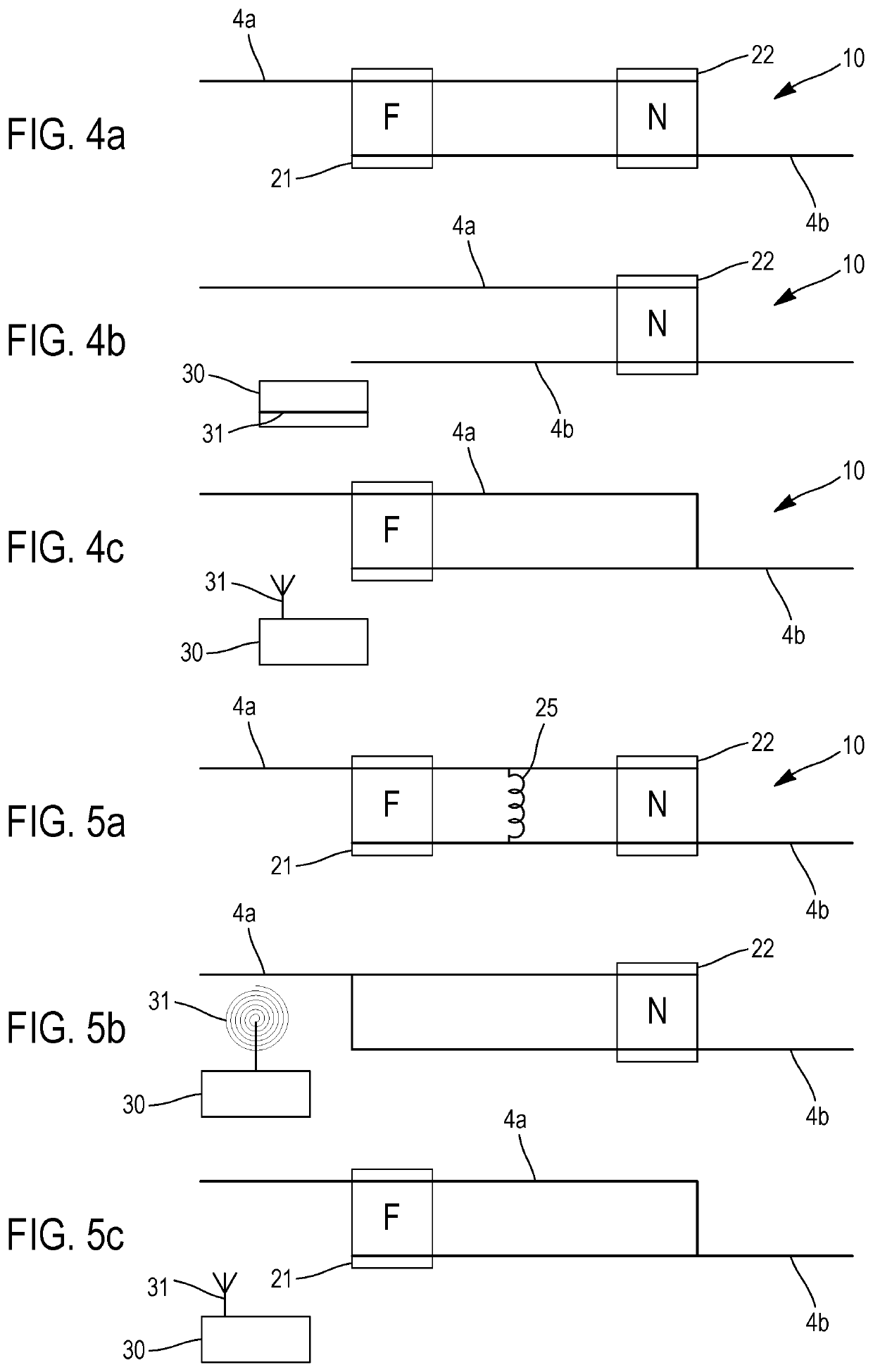
[0069]FIG. 4a represents the transmission-reception device 10 according to the present disclosure. The device is configured in a way quite similar to what was presented in the general description.
[0070]In FIG. 4b, the equivalent electrical diagram of device 10 in FIG. 4a is shown at the operating frequency of the second near-field chip 22. At this operating frequency, the first far-field chip 21 is passive, and its characteristic impedance being capacitive in nature, it constitutes an open circuit at the operating frequency of the second chip. In this configuration, the wire elements 4a, 4b electrically connected to the connection terminals of the second near-field chip 22 form transmission lines.
[0071]These transmission lines constitute the coupling device of the second near-field chip 22, capable of transmitting and receiving a radiofrequency electrical signal to another transmission line 31 of a transmission-reception terminal 30 located near the device 10. Preferably, to improve...
second embodiment
[0081]In a variant of this particularly advantageous second embodiment, the inductive element 25 is integrated into the first chip 21. This avoids the need to attach inductive element 25 separately between wire elements 4a and 4b. This variant can be implemented using a first chip 21, which integrates the inductive device 25 into a cover 7, for example, as shown in FIG. 7.
[0082]In order to promote electromagnetic coupling, the space between the two chips 21, 22 and forming at least part of the coupling device may be filled with a ferromagnetic material.
[0083]FIG. 8 shows a variant of the second embodiment. In this variant, the first chip 21 is associated with the wire elements 4a, 4b at longitudinal segments 4a1, 4b1 placed in the central parts of the wire elements 4a, 4b. The wire elements 4a, 4b therefore each have ends on either side of the first chip 21. The inductive element 25, which can be made in the form of a chip with connection areas, such as the grooves shown in FIG. 6, ...
PUM
 Abstract
Description
Claims
Application Information