Display device, display driver, and failure inspection method

a display device and failure inspection technology, applied in the field of display devices, display drivers, and failure inspection methods, can solve the problems of increased cost and device size, difficult to accurately detect failures, etc., and achieve the effect of accurately detecting failures in display panels, and reducing the size of devices

Active Publication Date: 2022-11-22
LAPIS TECH CO LTD
View PDF3 Cites 0 Cited by
  • Summary
  • Abstract
  • Description
  • Claims
  • Application Information

AI Technical Summary

Benefits of technology

[0013]In the present invention, failure inspection is performed using a plurality of operational amplifiers, which supply the output voltage generated by amplifying the drive voltage based on the image signal to the plurality of source lines of the display panel. In other words, the test voltage for failure inspection is supplied by one operational amplifier to the source lines, and the monitor voltage is acquired as test results by another operational amplifier. By acquiring the monitor voltages at respectively different timings and binarizing the monitor voltages it is possible to attain the failure determination signals that enable determination of the failure state.
[0014]As a result, it is possible to perform failure inspection for each of the source lines without providing an input circuit specifically for supplying a test voltage for failure inspection to the source lines or a comparison circuit for comparing the output result based on the test voltage to an expected value.
[0015]Additionally, in the present invention, failure determination is performed by acquiring monitor voltages (output results) attained by supplying the test voltage to the source lines at different timings and binarizing the monitor voltages. As a result, it is possible to accurately detect not only disconnection failures and short-circuit failures but also minute current leakage failures.
[0016]Thus, according to the present invention, it is possible to accurately detect failures occurring in the display panel while mitigating an increase in device size.

Problems solved by technology

Thus, in order to achieve the failure inspection disclosed in WO / 2018 / 079636, it is necessary to provide a comparison circuit for comparing the monitor output signal to the expected value within the source driver, which poses the issue of increased cost and device size.
Additionally, with the failure inspection disclosed in WO / 2018 / 079636, a failure is determined to have occurred by performing a size comparison using the expected value as a threshold, and thus, it has been difficult to accurately detect failures such as minute current leaks.

Method used


Image

  • Display device, display driver, and failure inspection method
  • Display device, display driver, and failure inspection method
  • Display device, display driver, and failure inspection method

Examples


embodiment 1

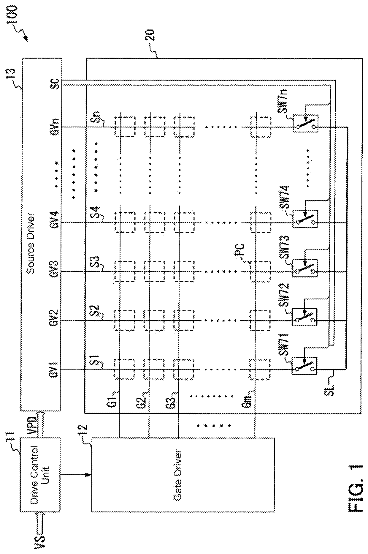
[0038]FIG. 1 is a block diagram showing a configuration of a display device 100 according to Embodiment 1 of the present invention.

[0039]The display device 100 has a drive control unit 11, a gate driver 12, a source driver 13, and a capacitive display panel 20.

[0040]The display device 20 has disposed therein gate lines G1 to Gm (m being an integer of 2 or greater) that each extend in the horizontal direction on a 2-dimensional screen, and source lines S1 to Sn (n being an integer of 2 or greater) that each extend in the vertical direction on the 2-dimensional screen, the gate lines and the source lines intersecting each other. Each intersection point between the gate line and the source line has formed therein a display cell PC as a liquid crystal element or an organic EL element, for example.

[0041]Additionally, the display panel 20 has disposed therein source line linking switches SW71 to SW7n that are connected respectively to the first end of each of the source lines S1 to Sn, an...

embodiment 2

[0122]FIG. 8 is a block diagram showing a configuration of a display device 100A according to Embodiment 2 of the present invention.

[0123]The display device 100A has a drive control unit 11, a gate driver 12, a source driver 13A, and a display panel 20A.

[0124]The drive control unit 11 and the gate driver 12 are the same as those shown in FIG. 1, and thus, explanations of operations thereof are omitted.

[0125]The display panel 20A differs from the display panel 20 shown in FIG. 1 by omitting the source line linking switches SW71 to SW7n, the linking line SL, and the wiring lines for the linking control signal SC, and otherwise has the same configuration as the display panel 20.

[0126]Similarly to the source driver 13 shown in FIG. 1, the source driver 13A generates n output voltages GV1 to GVn for each horizontal scanning period on the basis of the image data signal VPD supplied from the drive control unit 11, and supplies each of the output voltages GV1 to GVn to the source lines S1 t...

embodiment 3

[0166]FIG. 12 is a block diagram showing a configuration of a display device 100B according to Embodiment 3 of the present invention.

[0167]The display device 100B has a drive control unit 11, a gate driver 12, a source driver 13B, and a display panel 20A.

[0168]The drive control unit 11, the gate driver 12, and the display panel 20A are the same as those shown in FIG. 8, and thus, explanations thereof are omitted.

[0169]Similarly to the source driver 13A shown in FIG. 8, the source driver 13B generates n output voltages GV1 to GVn for each horizontal scanning period on the basis of the image data signal VPD supplied from the drive control unit 11, and supplies each of the output voltages GV1 to GVn to the source lines S1 to Sn of the display panel 20A.

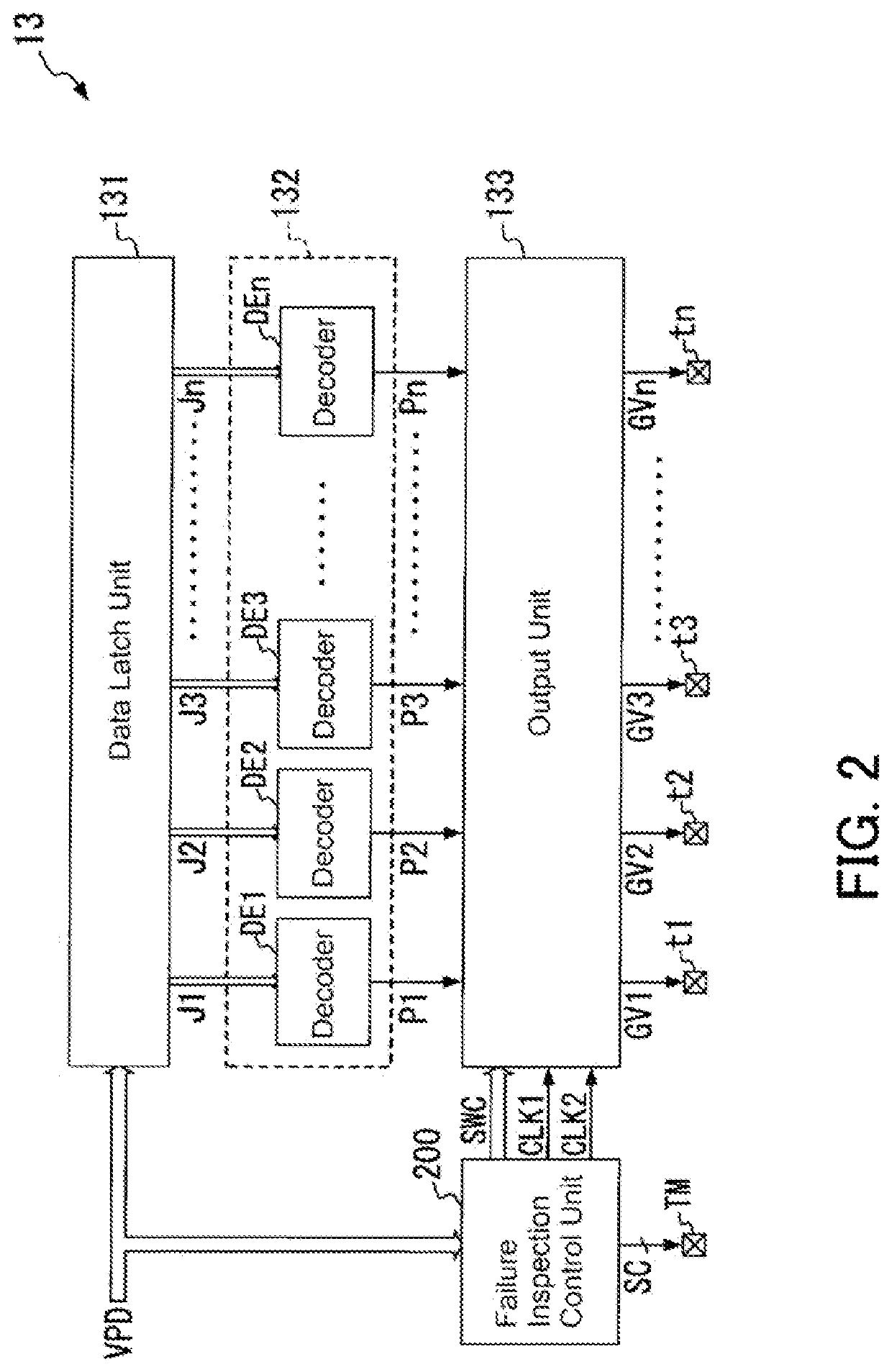
[0170]FIG. 13 is a block diagram showing an example of an internal configuration of the source driver 13B.

[0171]The source driver 13B includes a data latch unit 131, a decoder unit 132, an output unit 133B, and a failure inspection contr...


PUM


Abstract

An operational amplifier has a first input terminal and an output terminal connected to a second input terminal of the operational amplifier, and output nodes connected to the source lines of a display panel. During a failure inspection mode, the connection between the output node and the output terminal of the operational amplifier included in another output circuit among one output circuit and the other output circuit is disconnected and the output node instead of the output terminal is connected to the second input terminal of the operational amplifier. A pair of source lines connected to the output nodes of the one output circuit and the other output circuit are linked to each other, and signals attained by acquiring and binarizing voltages outputted from the operational amplifier in the other output circuit as a monitor voltage at different timings are acquired as first and second failure determination signals.

Description

CROSS REFERENCE TO RELATED APPLICATION[0001]This application is based upon and claims the benefit of priority of the prior Japanese Patent Application No. 2021-056891, filed on Mar. 30, 2021, the entire contents of which are incorporated herein by reference.TECHNICAL FIELD[0002]The present invention relates to a display device that displays an image according to an image signal, a display driver, and a failure inspection method.BACKGROUND ART[0003]In recent years, vehicles have been developed in which display panels such as liquid crystal display panels and organic EL (electroluminescence) display panels are used not only for car navigation systems but also to display various instruments. In this case, if there is a failure in the display panel used for the various instruments that results in erroneous display while the vehicle is in motion, this can pose the risk of impediments to driving.[0004]In order to handle this issue, a liquid crystal display device that includes a failure i...

Claims


Application Information

Patent Timeline
Patent Type & Authority Patents(United States)
IPC IPC(8): G09G3/20
CPCG09G3/20G09G2310/0291G09G2330/12G09G3/006G09G3/3208G09G3/36G01R31/52G01R31/54G01R31/56B60R11/0235B60R2011/0005G09G2310/0275
Inventor ICHIKURA, HIROYOSHI
Owner LAPIS TECH CO LTD
Why Eureka
Try Eureka