Method and system for supervising reference wafers on semiconductor device production line and recording medium

a technology of reference wafers and production lines, applied in the direction of process and machine control, instruments, computer control, etc., can solve the problems of product lot processing in the same set as the reference wafers, prone to occurrence of mistaken noting or failure noting, and troublesome operation

Inactive Publication Date: 2001-07-05
NEC ELECTRONICS CORP
View PDF0 Cites 10 Cited by
  • Summary
  • Abstract
  • Description
  • Claims
  • Application Information

AI Technical Summary

Benefits of technology

0022] It is yet another object of the present invention to provide a production control system and method for enabling the processing of a product lot to be halted immediately if the measured results of a reference wafer is negative, and a program product therefor.

Problems solved by technology

In the above-described conventional system, the management of the reference wafer lot and the product lot are supervised by an operator by noting down on a memo etc., at the time of delivery form the storage shelf, such operation being troublesome and liable to occurrence of mistaken noting or failure in noting.
If the measured data for the reference wafer is not good (NG), the operation of identifying the product wafers belonging to the product lot processed simultaneously with the reference wafer from the memo is time-consuming, such that there is a risk of the product lot processed in the same set as the reference wafer be introduced into the next process.
Moreover, if the product lot processed in the same set as the reference wafer could be identified e.g., from the memo, it is not so easy to halt the progress of the process for the product lot.
The reason is that, since the reference wafer is discarded after processing in the wafer process device and measurement in the measurement device, in distinction from the product lot, the conventional production control system is not provided with the function of supervising the correspondence between the reference wafer and the product lot, and that it is extremely difficult to check whether or not the product lot being transported by e.g., an unmanned transporting car to the next step after processing in the wafer process device is the product lot processed in the same set as the reference wafer.
If the measured result in the reference wafer measurement device is to be checked manually, and if the measured result of the reference wafer is NG, it is difficult to halt the progress of the product lot process immediately, by the same reason as discussed above.

Method used


Image

  • Method and system for supervising reference wafers on semiconductor device production line and recording medium
  • Method and system for supervising reference wafers on semiconductor device production line and recording medium
  • Method and system for supervising reference wafers on semiconductor device production line and recording medium

Examples


Embodiment Construction

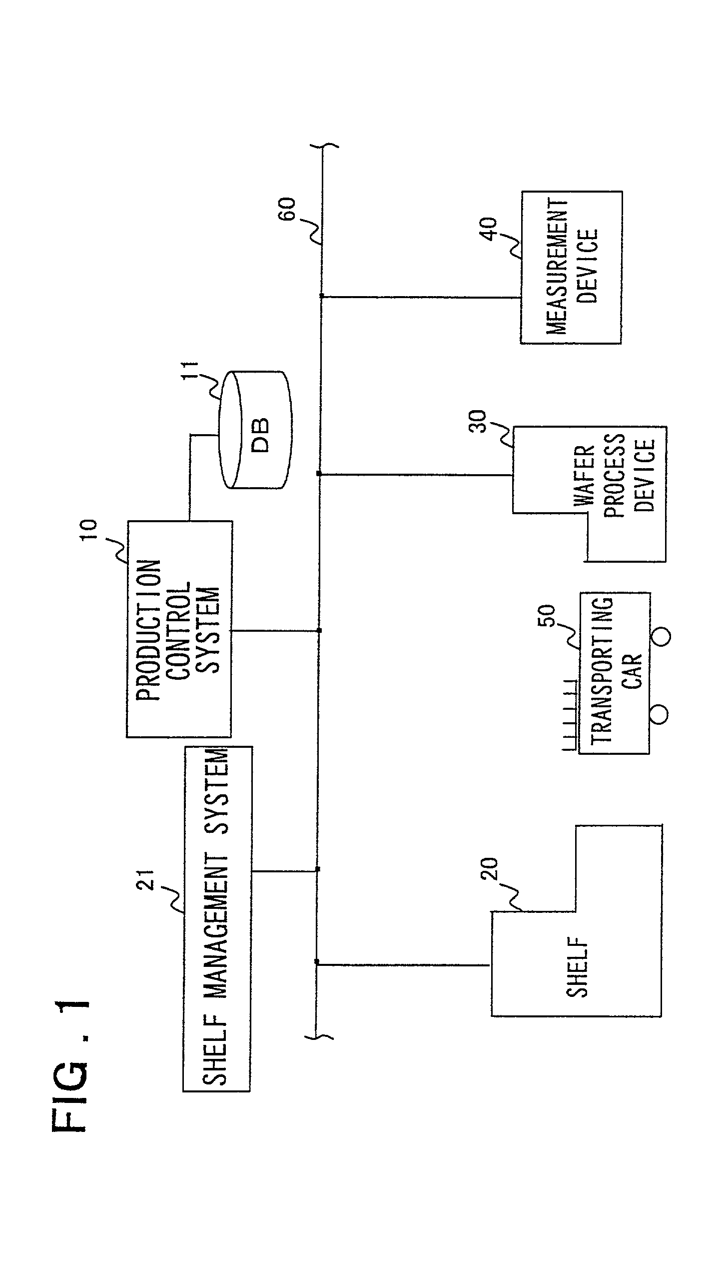
[0055] In the following certain preferred embodiments of the present invention are explained. In a preferred embodiment of the present invention, there is provided means for affording reference wafers with a preset common representative name at the time of charging (introducing) thereof and for changing the item name of the reference wafers from the representative name into an item name conforming to the processing condition.

[0056] In a preferred embodiment of the present invention, the charged (introduced) plural reference wafers are afforded with a common representative name and holds it during warehousing to and delivery from the shelf and during transport.

[0057] So, it is unnecessary to sort the plural reference wafers stored on the shelf according to processing conditions in the wafer process device, such that the reference wafers are stored collectively on the storage shelf. In this preferred embodiment of the present invention, the operation of searching for a shelf matched t...


PUM


Abstract

Provision of a shelf management system and method for semiconductor devices enabling efficient use of a reference wafer storage shelf and also enabling stop of process progress of product lot in case of unusual data representing reference wafer measurement results. A production control system responsible for supervision of a production line has a function of changing the reference wafer item name. The production control system accords a preset common representative name to plural reference wafers. Upon warehousing plural reference wafers to a storage shelf, the reference wafers are collectively stored in a storage shelf, without classification according to processing conditions in the wafer process device where the reference wafers are to be processed. The item name is changed to a name corresponding to the processing conditions at the time of processing the reference wafers in the wafer process device.

Description

[0001] This invention relates to a production control system for semiconductor devices and, more particularly, to a system and a method for supervising reference wafers in a semiconductor device production process, and to a program product.[0002] A reference wafer used for testing, evaluation, maintenance and inspection, is processed under a preset condition along with a product wafer in an oxidation device, a diffusion device, a CVD device or in an epitaxial growth device, referred to below as a wafer process device, in e.g., an oxide film forming step, a thermal diffusion process, a CVD process or in an epitaxial growth process. After the end of the processing, the film thickness of the reference wafer, for example, is measured by a film thickness measurement device to check whether or not the reference wafer will behave satisfactorily in the wafer process device.[0003] Up to now, in a production line for semiconductor devices, a preset number of item names are provided on the sid...

Claims


Application Information

Patent Timeline
Patent Type & Authority Applications(United States)
IPC IPC(8): G05B15/02H01L21/00H01L21/02H01L21/68
CPCH01L21/67276H01L21/68
Inventor SUGIKAWA, YUTAKA
Owner NEC ELECTRONICS CORP
Why Eureka
Try Eureka