Signal processing semiconductor integrated circuit device

Inactive Publication Date: 2001-08-30
HITACHI LTD
View PDF0 Cites 11 Cited by
  • Summary
  • Abstract
  • Description
  • Claims
  • Application Information

AI Technical Summary

Benefits of technology

[0017] It is thus an object of the present invention to provide a signal-processing semiconductor integrated circuit that is used in a radio-communication system for signal processing to convert the frequency of a received signal (or a desired signal) into a lower frequency by mixing the received signal with a local oscillation signal, and is capable of reducing a CN ratio's deterioration caused by a spurious noise.
[0036] If there is further provided a third mixer circuit for converting the frequency of a signal generated as a result of the frequency conversion carried out by the first mixer circuit by mixing the signal with the second oscillation signal generated by the second oscillation circuit in a second-stage frequency conversion, it is preferable to separate the first group of circuits comprising the first mixer circuit and the first oscillation circuit from a third group of circuits comprising the second oscillation circuit, the amplification circuit, the demodulation circuit and the third mixer circuit. In this case, it is also nice to place one of the second mixer circuit, the oscillation control circuit, the modulation circuit and the control circuit or any combination of the second mixer circuit, the oscillation control circuit, the modulation circuit and the control circuit between the first group of circuits and the third group of circuits. In this way, even for a signal-processing LSI employed in a radio-communication system adopting the double super-heterodyne technique, it is possible to reduce the amount of wasted space on the semiconductor substrate and to reduce the deterioration of the CN caused by a spurious noise.

Problems solved by technology

Thus, reduction of the component count is a technological challenge of importance.
To put it concretely, the result of the test indicated that, when an interference wave with an interfering frequency was introduced at -26 dB to a desired signal input through the antenna at -99 dB, the CN ratio deteriorated, causing a bit error rate to exceed a desirable level.

Method used


Image

  • Signal processing semiconductor integrated circuit device
  • Signal processing semiconductor integrated circuit device
  • Signal processing semiconductor integrated circuit device

Examples


Embodiment Construction

[0051] Preferred embodiments of the present invention are explained by referring to the diagrams as follows.

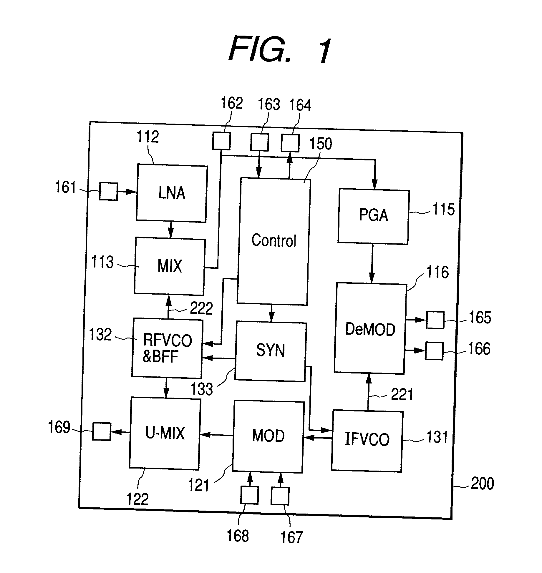
[0052] FIG. 1 is an explanatory diagram referred to in a description of a layout of an embodiment applying the present invention to a signal-processing semiconductor integrated circuit employed in a radio-communication system adopting a single super-heterodyne technique. The signal-processing semiconductor integrated circuit comprises the circuit blocks shown in FIG. 11. To be more specific, a single chip 200 implementing the signal-processing semiconductor integrated circuit includes the reception-system circuit 110 (excluding the band-limiting filter (FLT) 111 and the band-pass filter (BPF) 114), the transmission-system circuit 120 (excluding the power amplifier (PA) 123, the oscillation-system circuit 130 and the system controller 150). The layout of the circuit blocks is devised to reduce the number of spurious noises. The band-limiting filter (FLT) 111 and the band-pass f...


PUM


Abstract

A semiconductor integrated circuit comprising a first circuit block including an oscillation circuit considered to be a noise generator and a second circuit block including circuits considered to be easily affected by a noise generated by the oscillation circuit, being most likely led to a malfunction are created on a single semiconductor substrate with the first and second circuit blocks separated from each other. To put it more concretely, the first and second circuit blocks are respectively created in a first island area and a second island area on the surface of the semiconductor substrate. The first and second island areas are each enclosed by an insulating isolation band. A low-resistance semiconductor area is created in a base area excluding locations occupied by active elements in the first and second island areas and is connected to a stable voltage terminal.

Description

BACKGROUND OF THE INVENTION[0001] The present invention relates to a technology of reducing cross talk in a semiconductor integrated circuit and a technology effectively applicable to a signal-processing LSI (or a large-scale semiconductor integrated circuit) for receiving and processing signals in a plurality of different frequency bands. More particularly, the present invention relates to a technology effectively applicable to a radio-communication LSI employed typically in a hand phone for processing a signal received by adoption of a super-heterodyne technique.[0002] As a radio-communication system adopted in a hand phone, there is known a radio-communication system embracing the super-heterodyne technique as shown in FIG. 11. In the radio-communication system shown in FIG. 11, reference numeral 100 denotes an antenna for receiving a signal wave and reference numeral 101 denotes a reception / transmission changeover switch. Reference numeral 110 denotes a reception-system circuit ...

Claims


Application Information

Patent Timeline
IPC IPC(8): H01L27/04H01L21/762H01L21/822H01L27/06H04B1/18H04B1/38H04B1/3822
CPCH01L21/76264H01L27/0623H01L2924/0002H01L2924/00H04B1/18
Inventor KASA, NOBUHIROTASHIRO, YOSHIYASUHORI, KAZUAKI
Owner HITACHI LTD
Why Eureka
Try Eureka