Method for forming conductive bumps for the purpose of contrructing a fine pitch test device

a test device and conductive bump technology, applied in the direction of individual semiconductor device testing, semiconductor/solid-state device testing/measurement, instruments, etc., can solve the problems of high cost of die sum, low yield rate of such mcms, and incomplete packag

Inactive Publication Date: 2002-01-31
EPITECH +1
View PDF0 Cites 220 Cited by
  • Summary
  • Abstract
  • Description
  • Claims
  • Application Information

AI Technical Summary

Problems solved by technology

Yield rates for such MCMs are usually low because if any one of the die within a MCM malfunctions, the entire package is considered defective.
Because the sum cost of the die can be quite expensive, the production of MCMs is frequently unprofitable and the cost to the consumer of MCMs is frequently unjustifiable.
Such a process is labor intensive and expensive and still could result in uncertainty in determining whether a die is a "known good die."
These tests, however, only certify that a die is good at this stage in its manufacturing cycle.
A problem with the above device and test methods is the utilization of rigid metal probes or probes with rigid metal tips for establishing electrical continuity.
Such probes are difficult to manufacture and require high maintenance.
Because the individual probes are so minute, the practical difficulties of using probe cards include keeping the probes straight, keeping them at an even or planar height, and establishing electrical contact through all of the probes in the proper location simultaneously without exerting so much pressure on the semiconductor wafer that it is damaged.
Additionally, the mere act of establishing electrical contact with the proper points within a circuit can be a challenging task.
Another problem with using probe cards as disclosed by Leedy is that they typically have inherent frequency response characteristics which inhibit full functional testing of an integrated circuit throughout the desired frequency ranges.
Thus, the cards cannot be used to test the overall reliability of the bare die to determine whether the die will work for a significant duration of time.
Neither do they provide a means for testing the die over a broad range of temperatures.
A problem with such a device is that it is very difficult to manufacture bumps such that pad to bump contact is established for all die bond pads because of the rigidness of the solder microbumps.
In other words, use of such bumps introduces planarity problems.
Furthermore, the use of such bumps does not insure solid and continuous electrical contact with the bare die bond pads.
Additionally, the frequency bandwidth is limited.
Thus, these metal bumps do not support all of the types of required tests which may have to be performed even if they do successfully establish electrical continuity with the die bond pads.
One problem with such an implementation is the difficulty of plating the small microbumps; the disclosure does not adequately disclose the method of plating the microbumps.
A second technical problem is the establishing of electrical continuity between the plated bumps and the pads of a substrate or test socket....

Method used


Image

  • Method for forming conductive bumps for the purpose of contrructing a fine pitch test device
  • Method for forming conductive bumps for the purpose of contrructing a fine pitch test device
  • Method for forming conductive bumps for the purpose of contrructing a fine pitch test device

Examples


second embodiment

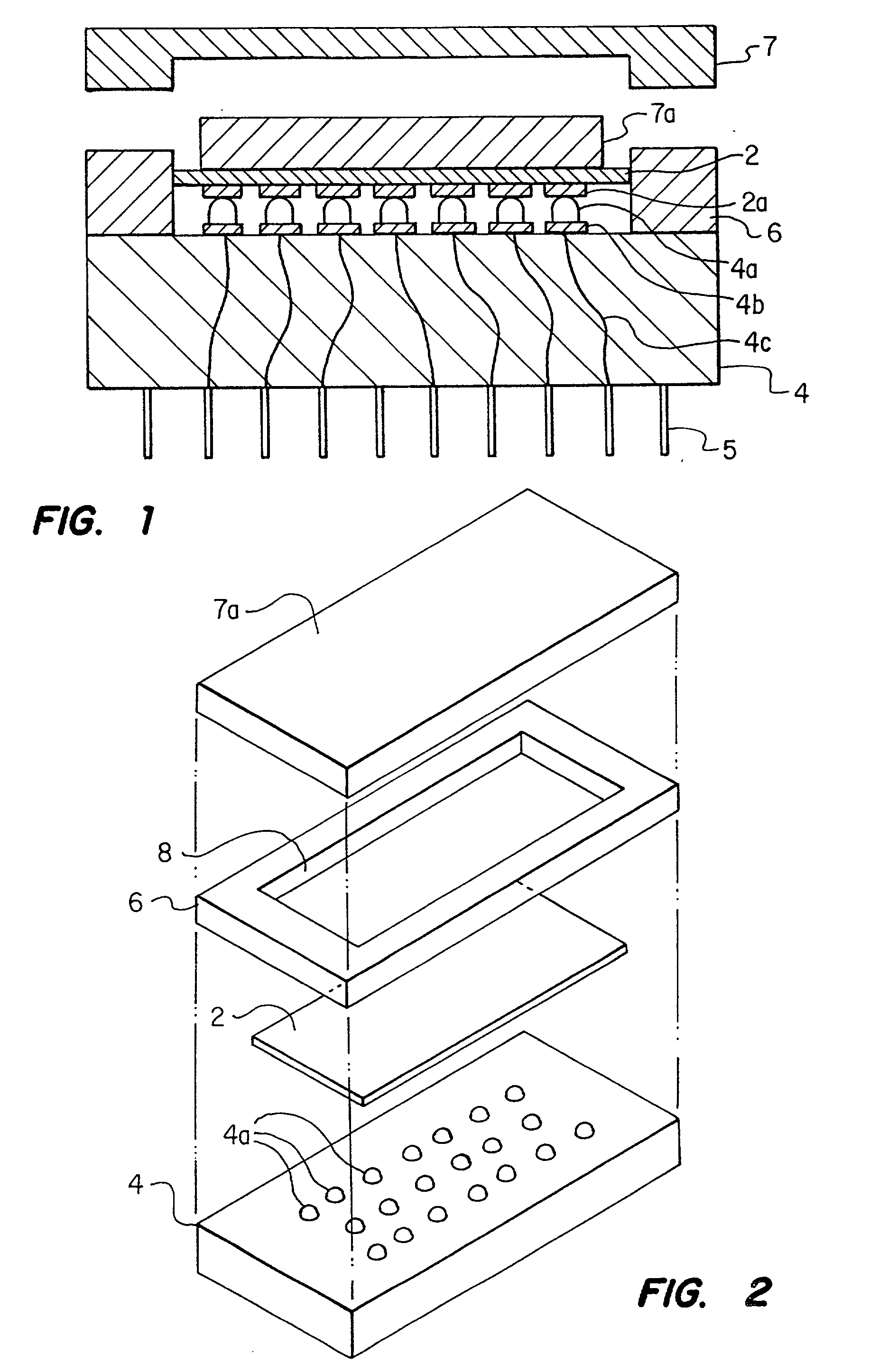
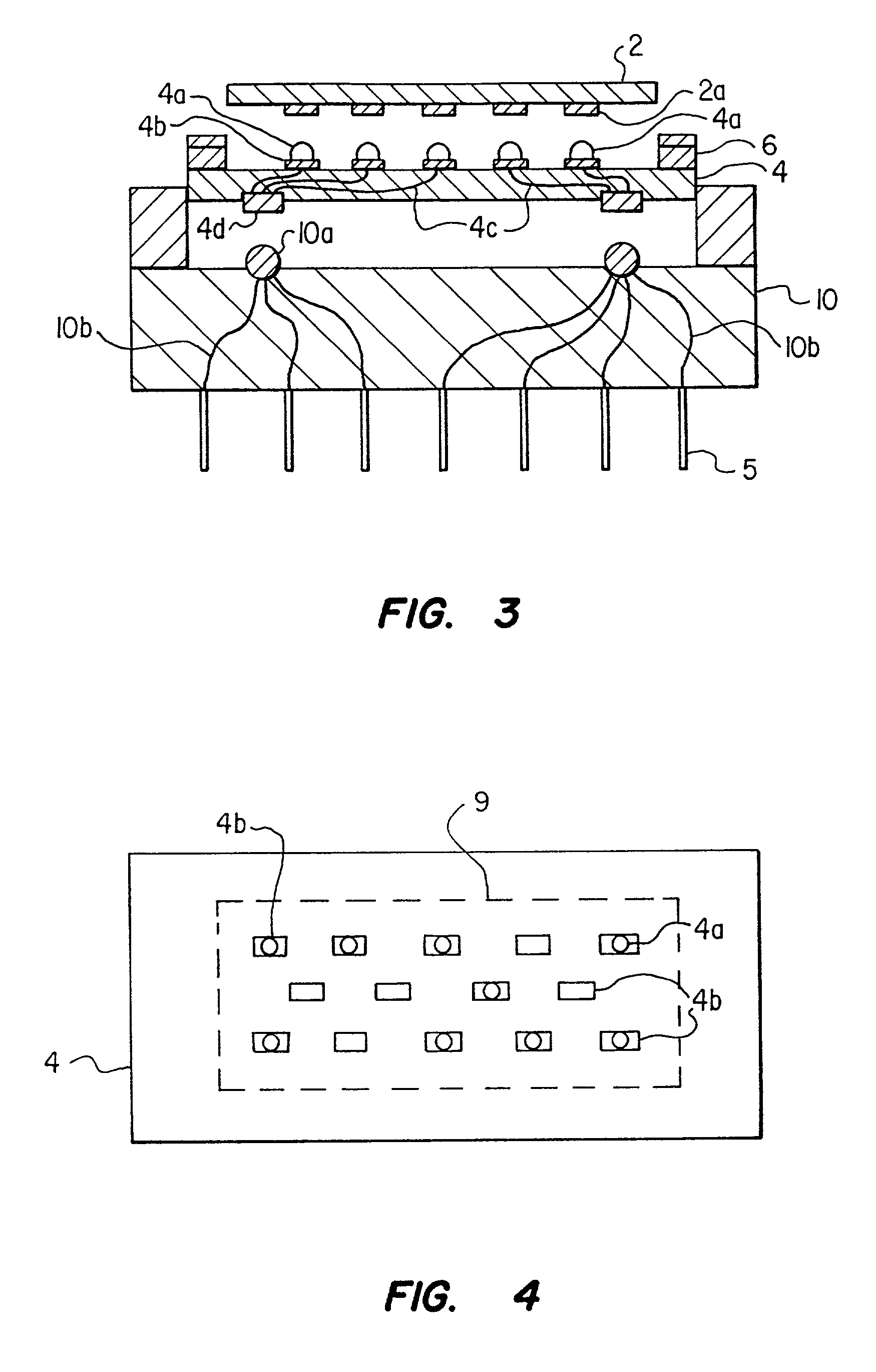
[0052] In the means for connecting, as is shown in FIG. 3, a die carrier 4 mates with a carrier connector 10. The circuit pads 4b of the die carrier 4 are placed upon its top surface while its connection pads 4d are placed on its bottom side. The carrier connector's connection pads 10a are individually connected to the leads 5 of the carrier connector 10 through connection lines 10b.

[0053] The connection pads 4d of the die carrier 4 and the connection pads 10a of the carrier connector 10 can be arranged in any format. One good arrangement is to have a row of connection pads 4d of the die carrier 4 at each end of the die carrier 4. The carrier connector 10 contains a similar arrangement wherein the row of the carrier connector's connection pads 10a on the carrier connector 10 is designed to make electrical contact with the row of connection pads 4d of the die carrier 4. The arrangement of carrier connector's connection pads 10a is immaterial so long as the placement corresponds with,...

third embodiment

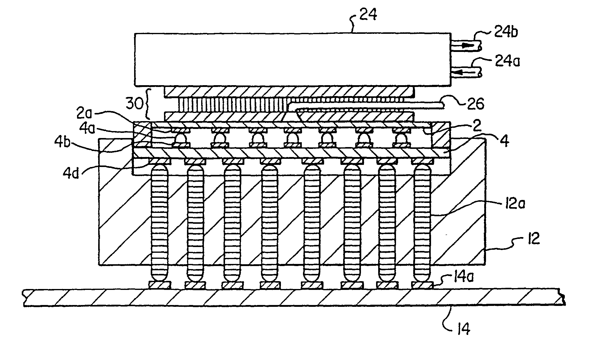
[0054] In the means for connecting, as is shown in FIG. 5, a surface mounted carrier connector 12 is mounted to the surface of a burn-in board 14 (or "mother board"). However, instead of utilizing metal pins (not shown) which must be soldered to the burn-in board 14, this surface mounted carrier connector 12 uses an elastomeric interconnection lead 12a, as disclosed by U.S. Pat. No. 5,074,947, to establish electrical continuity between the burn-in board connection pads 14a and the bottom connection pads 4d of a die carrier 4. Use of this type of carrier connector for surface mount applications is advantageous because of lower labor cost in installing it when compared to the carrier connector 12 or any other device utilizing metal leads 5 which require soldering of individual leads 5. Further, the elastomeric interconnect leads 12a have an increased frequency bandwidth in comparison to the thin metallic leads 5a of the standard carrier connector.

[0055] Referring again to FIG. 2, the ...


PUM


Abstract

A system is described for using with fine pitch devices including singulated bare die, semiconductor wafers, chip sized packages, printed circuit boards, and the like to determine that the fine pitch device is not faulty. The system is also usable for transfer of data, energy, for collecting data measurements or measurement-related data between two pieces, and for effecting at least part of an identification process. The disclosed embodiment includes a substrate having a circuit pad pattern in the mirror image of the pattern of contact points, usually bond pads of the fine pitch device to be connected. A conductive elastomeric probe is permanently formed on the circuit pads of the substrate such that the probe is malleable and allows repetitive electrical contact. The system may also contain an alignment template for orienting the fine pitch device onto the elastomeric probes of the contact point pattern of the substrate.

Description

[0001] 1. Technical Field of the Invention[0002] This invention relates to a method and apparatus of making and using a reusable system for establishing a contact with a variety of fine pitch devices, for example, unpackaged semiconductor devices, semiconductor wafers, bare and populated printed circuit boards, and other fine pitch devices such as chip-scale packages and ball-grid array packages.[0003] 2. Description of Related Art[0004] Multi-chip Modules (MCMs), or Hybrid Integrated Circuits, are manufactured by combining multiple integrated circuit dies within one package. Yield rates for such MCMs are usually low because if any one of the die within a MCM malfunctions, the entire package is considered defective. For example, MCMs which contain 20 individual die, with an average yield rate of 97.3% would be expected to have an overall yield rate of 57.3% because of the cumulative effect of the individual yield rates of each die. Because the sum cost of the die can be quite expens...

Claims


Application Information

Patent Timeline
IPC IPC(8): G01R1/073G01R31/02G01R31/28H01L21/50H01L21/66
CPCG01R1/0483G01R1/0735
Inventor SMITH, KENNETH R.PIERCE, JOHN L. JR.
Owner EPITECH
Why Eureka
Try Eureka