Plasma display panel and plasma display panel manufacturing method for achieving improved luminescence characteristics
a technology of plasma display panel and manufacturing method, which is applied in the field of plasma display panel and plasma display panel manufacturing method for achieving improved luminescence characteristics, can solve the problems of reducing the luminous intensity, deteriorating the luminescence characteristics, and reducing the use of phosphors
- Summary
- Abstract
- Description
- Claims
- Application Information
AI Technical Summary
Benefits of technology
Problems solved by technology
Method used
Image

Examples
first embodiment
[0065] First Embodiment
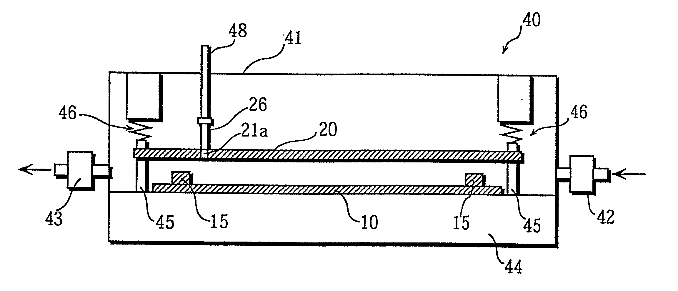
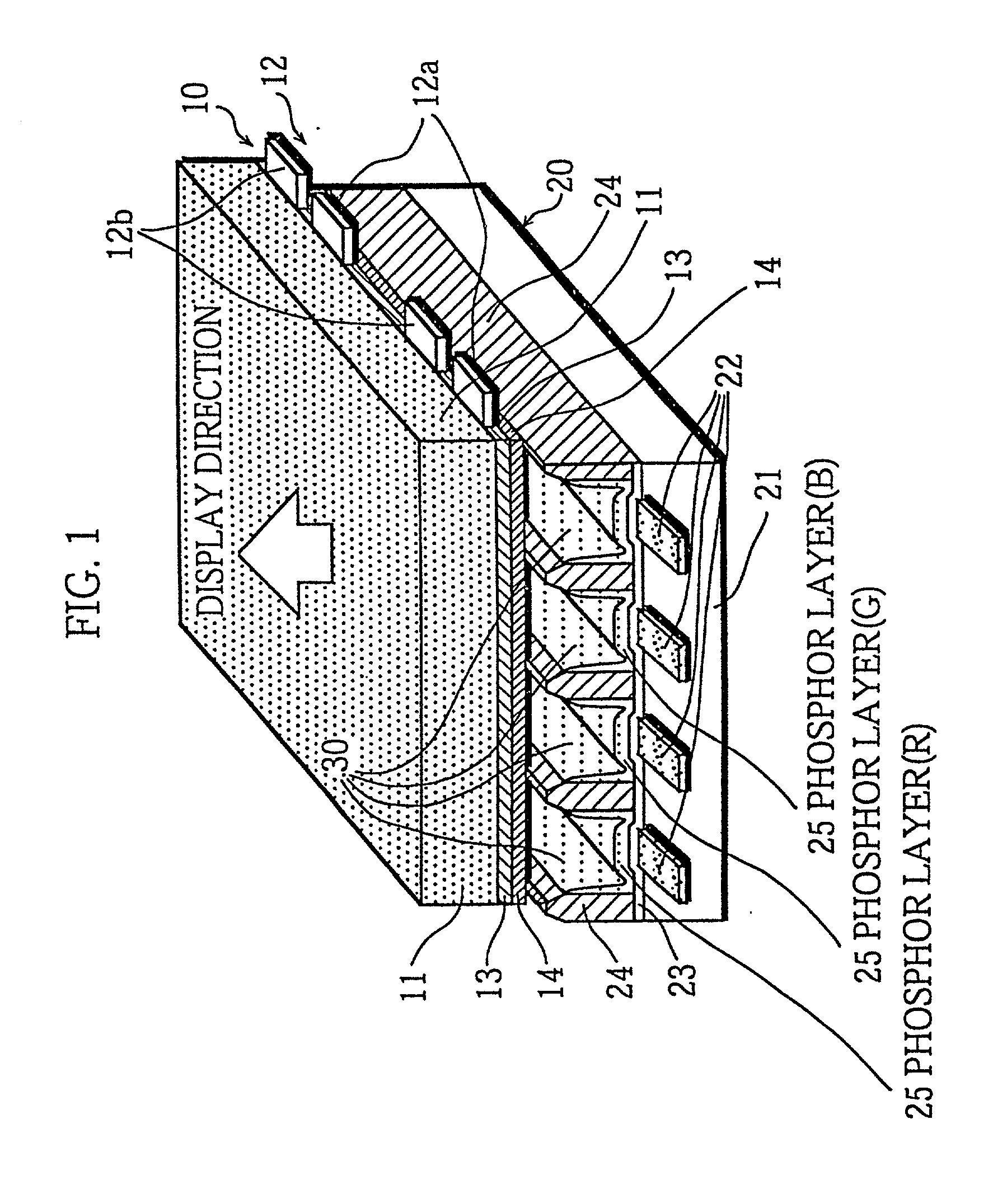
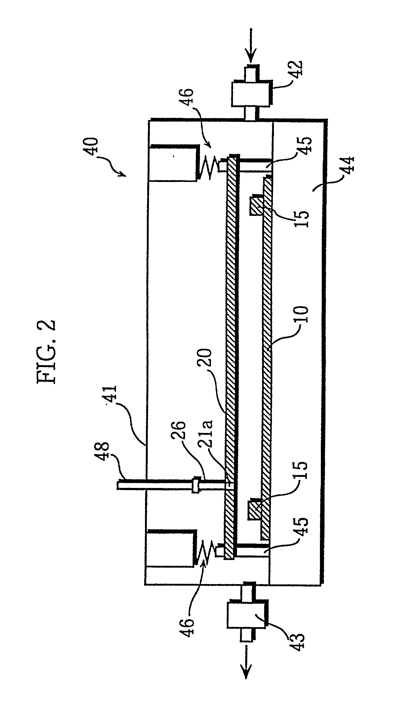
[0066] FIG. 1 is a cross-section showing the essential components of an AC PDP relating to the present embodiment. In the drawing, a part of the display area in the center of the PDP is shown.
[0067] This PDP is constructed from a front plate 10 and a back plate 20. The front plate 10 is formed from a front glass plate 11, on whose inward surface are placed discharge electrodes 12, formed of pairs of scanning electrodes 12a and sustaining electrodes 12b, a dielectric layer 13 and a protective layer 14. The back glass plate 20 is formed from a back glass plate 21, on whose inward surface are placed address electrodes 22 and a visible light reflective layer 23. The front plate 10 and the back plate 20 are arranged in parallel leaving a gap between them, with the discharge electrodes 12 and the address electrodes 22 facing each other. The space between the front plate 10 and the back plate 20 is divided into discharge spaces 30 by constructing partitions 24, which...
second embodiment
[0177] Second Embodiment
[0178] In this embodiment, the aging process and subsequent processes differ from those in the first embodiment, but the structure of the PDP and the manufacturing method used are identical, so that only those points unique to this embodiment will be explained here.
[0179] In the present embodiment, after the front and back plates have been sealed, the aging process is performed under the conditions normally prevailing in the related art. This method is a simple one, in which a pulse discharge is applied between discharge electrodes to generate a discharge. However, in this conventional aging process, heat deterioration in the phosphors as described above causes a marked deterioration in the luminous intensity and discharge characteristics to occur. This embodiment aims to effectively restore the deterioration in the luminescence characteristics caused to the phosphor layer during the aging process.
[0180] With this aim in mind, the following additional process...
PUM
 Abstract
Description
Claims
Application Information
 - R&D
- Intellectual Property
- Life Sciences
- Materials
- Tech Scout
- Unparalleled Data Quality
- Higher Quality Content
- 60% Fewer Hallucinations
Browse by: Latest US Patents, China's latest patents, Technical Efficacy Thesaurus, Application Domain, Technology Topic, Popular Technical Reports.
© 2025 PatSnap. All rights reserved.Legal|Privacy policy|Modern Slavery Act Transparency Statement|Sitemap|About US| Contact US: help@patsnap.com