Wafer burn-in and test employing detachable cartridge

a detachable cartridge and wafer technology, applied in the field of wafers, can solve the problems of circuits (ic's), prone to fail early in their projected lives, and loss of added packaging costs,

Inactive Publication Date: 2002-03-14
AEHR TEST SYST
View PDF0 Cites 9 Cited by
  • Summary
  • Abstract
  • Description
  • Claims
  • Application Information

AI Technical Summary

Benefits of technology

[0013] Yet further according to the invention there is provided a kinematic coupling comprising a male connector including an undercut surface; and first and second opposed jaws. Each of the jaws is movable from a retracted position in which the male connector can be inserted between the jaws and an engaging position in which the jaws prevent withdrawal of the male connector from between the jaws by engaging the undercut surface of the male connector. Preferably the first and second jaws are biased towards their respective engaging positions, and the first and second jaws each include an inclined surface that can be acted upon by a key to move the first and second jaws into their respective retracted positions. More preferably, the male connector is movably coupled to a substrate such that, when the male connector is inserted between the first and second jaws and the first and second jaws are both in their engaging positions, the male connector is movable relative to the substrate between an extended position in which the engaging surface of the male connector is not in contact with the first and second jaws and a retracted position in which the engaging surface of the male connector is in contact with the first and second jaws. Even more preferably, the male connector is biased towards its retracted position, thereby to provide a positive clamping force.
[0018] at least one jaw that is movably coupled to the second plate, the jaw being movable from a retracted position in which the male connector can be received by the jaw and an engaging position in which the jaws prevent withdrawal of the male connector from the jaw by engaging the undercut surface of the male connector.

Problems solved by technology

It is well known that integrated circuits (IC's), if they are going to fail, tend to fail early in their projected lives.
To identify and eliminate such fragile IC's, IC manufacturers typically expose their integrated circuits to conditions that tend to induce such premature failure.
Disadvantages of burning-in packaged IC's are that the added expense of packaging the IC is lost if the IC fails during burn-in, that there are many more individual components to handle, and that the same die type may end up in a number of different package types requiring different fixtures for burn-in.
This method has the advantage that less has been invested in the IC at this time, but has the disadvantage that the individual dies are difficult to handle conveniently, and are susceptible to damage or contamination.
Wafer-level burn-in has the disadvantages that careful handling of the wafer is required, and that making electrical contact with the wafer is more difficult.

Method used


Image

  • Wafer burn-in and test employing detachable cartridge
  • Wafer burn-in and test employing detachable cartridge
  • Wafer burn-in and test employing detachable cartridge

Examples


Embodiment Construction

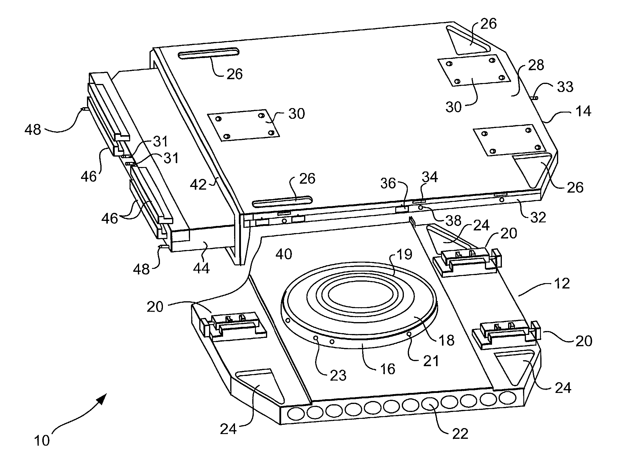
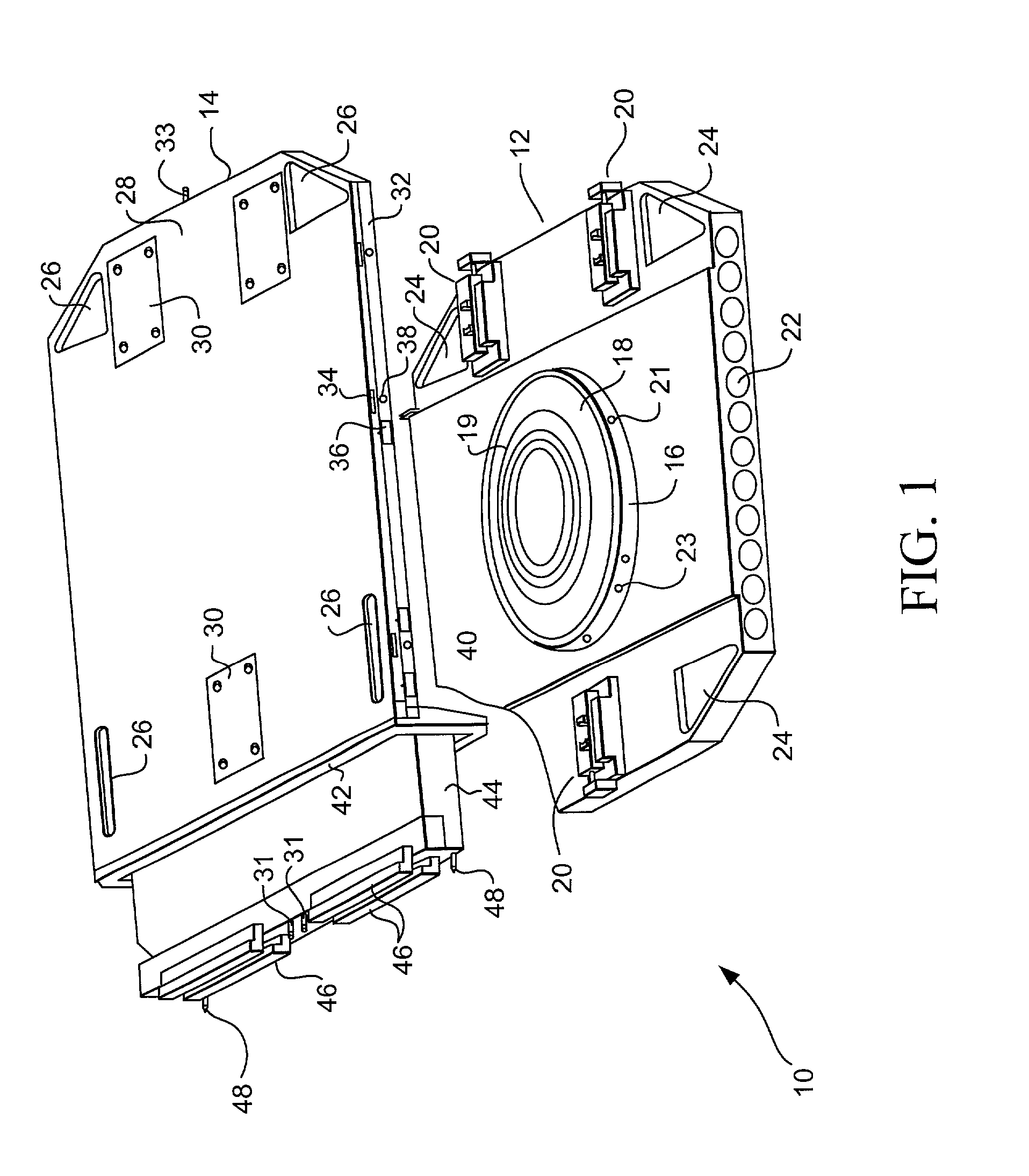
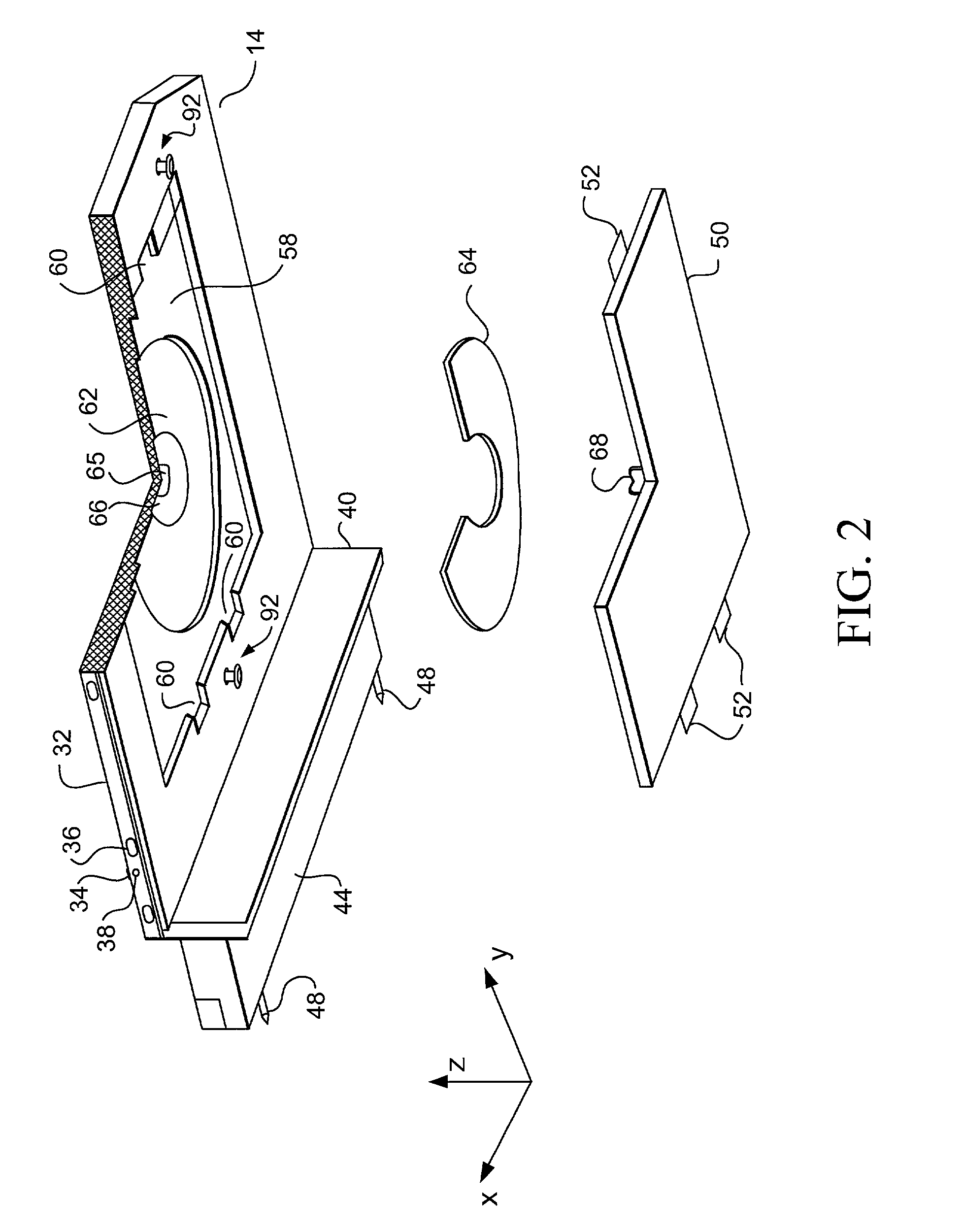
[0038] A wafer-level burn-in and test cartridge according to the invention is illustrated in FIG. 1. The cartridge, generally indicated by the reference numeral 10, comprises a chuck plate 12 and a probe plate 14. The chuck plate 12 and the probe plate 14 may be made of any suitable material. In the illustrated embodiment, the chuck plate 12 and the probe plate 14 are made of 6061 aluminum.

[0039] The chuck plate 12 is generally rectangular in shape, and includes a centrally-located raised pedestal 16. In use, a semiconductor wafer is placed on the upper surface 18 of the pedestal 16. Mounted to the upper surface of the chuck plate 12 are the lower halves 20 of three mechanical connecting devices that are used to lock the chuck plate 12 and the probe plate 14 together in use. In the illustrated embodiment, the mechanical connecting devices are kinematic couplings, which are discussed below in more detail with reference to FIGS. 6 to 12. Formed transversely through the chuck plate 12 ...


PUM


Abstract

A cartridge (10) includes a chuck plate (12) for receiving a wafer (74) and a probe plate (14) for establishing electrical contact with the wafer. In use, a mechanical connecting device (90) locks the chuck plate and the probe plate fixed relative to one another to maintain alignment of the wafer and the probe plate. Preferably, electrical contact with the wafer is established using a probe card (50) that is movably mounted to the probe plate by means of a plurality of leaf springs (52.) The mechanical connecting device is preferably a kinematic coupling including a male connector (94) and first and second opposed jaws (122, 124.) Each of the jaws is pivotable from a retracted position in which the male connector can be inserted between the jaws and an engaging position in which the jaws prevent withdrawal of the male connector from between the jaws. The male connector is movable between an extended and a retracted position, and is biased towards the retracted position. This provides a positive clamping force that pulls the chuck and probe plates together when the mechanical connecting device is engaged. To load a wafer into the cartridge, the wafer is placed on the chuck plate, the probe plate is aligned with the wafer, and the chuck plate and the probe plate are locked together. The cartridge can then be removed from the alignment device and placed in a burn-in or test chamber that does not itself require means for aligning the wafer or for providing a probe actuation force.

Description

[0002] 1. Technical Field[0003] This invention particularly relates to a cartridge for use in the burn-in and / or test of circuitry formed on semiconductor wafers, before the wafer is diced. The invention may however also be applicable to the burn-in or test of other electrical devices. This invention further relates to methods of loading and aligning a probe card in the cartridge with a semiconductor wafer located in the cartridge. The invention also relates to a connecting device for use in the cartridge. This invention is related to the inventions in commonly owned U.S. Pat. No. 5,429,510, issued to Barraclough et al. on Jul. 5, 1995, entitled "High-Density Interconnect Technique," and commonly owned U.S. Pat. No. 5,682,472, issued to Brehm et al. on Oct. 28, 1997 and entitled "Method and System for Testing Memory Programming Devices," the disclosures of which are hereby incorporated by reference herein. This invention is further related to the invention in a concurrently filed, c...

Claims


Application Information

Patent Timeline
Patent Type & Authority Applications(United States)
IPC IPC(8): G01R31/28
CPCG01R1/0408G01R1/0491G01R31/2831G01R31/2855G01R31/2863G01R31/2865G01R31/2886
Inventor UHER, FRANK OTTOANDBERG, JOHN WILLIAMCARBONE, MARK CHARLESRICHMOND, DONALD PAUL II
Owner AEHR TEST SYST
Why Eureka
Try Eureka