
Method of alignment for buried structures formed by surface transformation of empty spaces in solid state materials

a technology of solid-state materials and surface transformation, applied in semiconductor devices, semiconductor/solid-state device details, instruments, etc., can solve problems such as alignment target reading problems, alignment of various buried structures, and readability of marks

Inactive Publication Date: 2002-06-20
MICRON TECH INC
View PDF0 Cites 57 Cited by
  • Summary
  • Abstract
  • Description
  • Claims
  • Application Information

AI Technical Summary

Benefits of technology

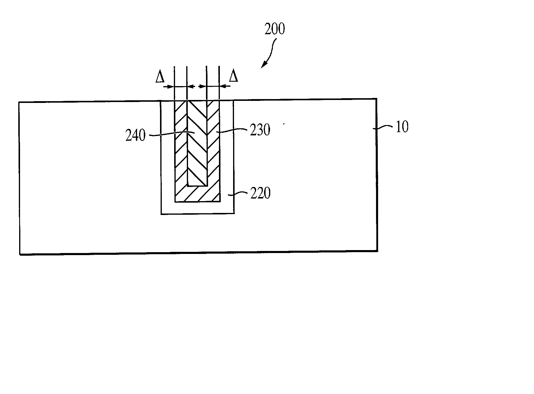
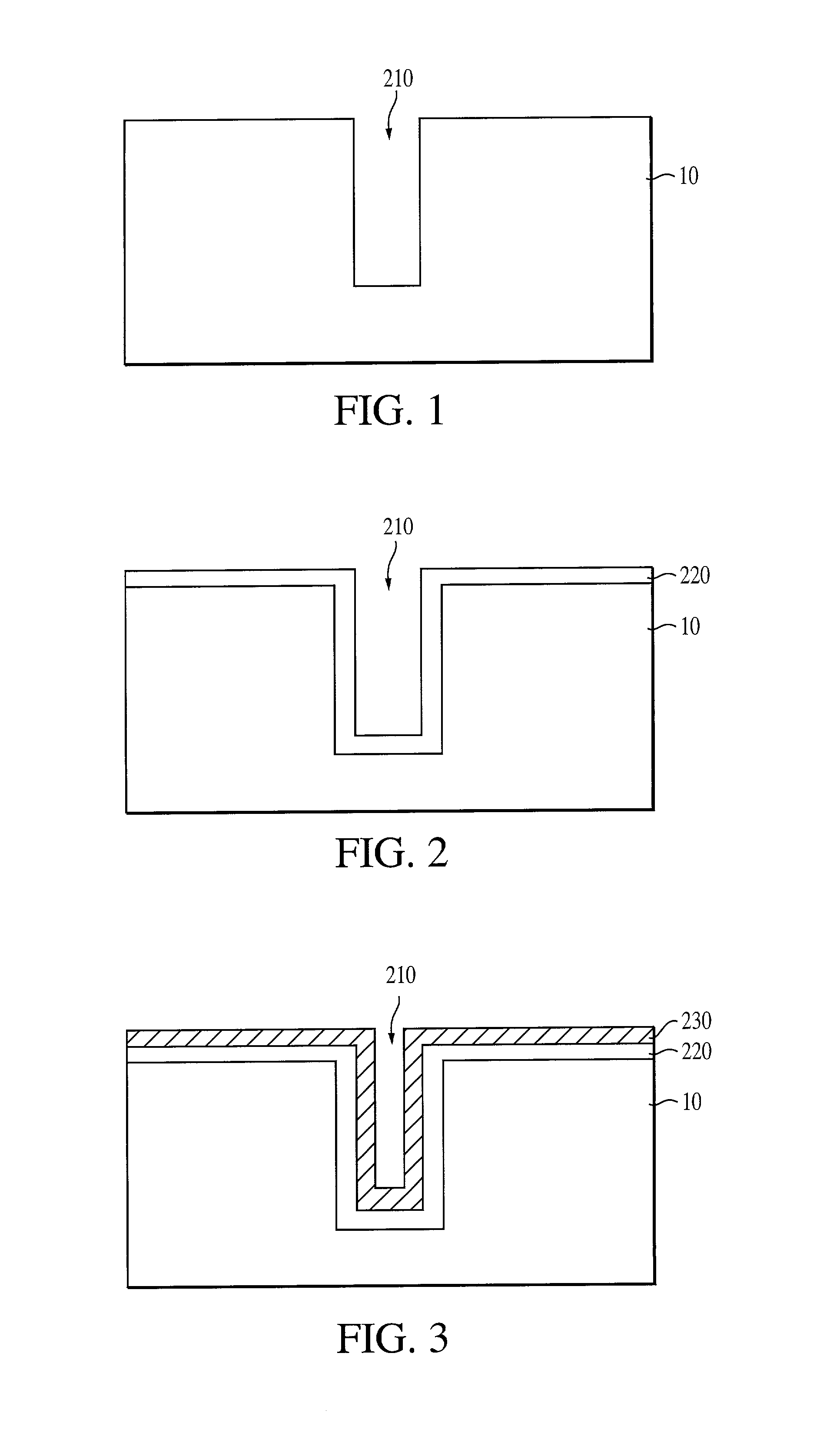
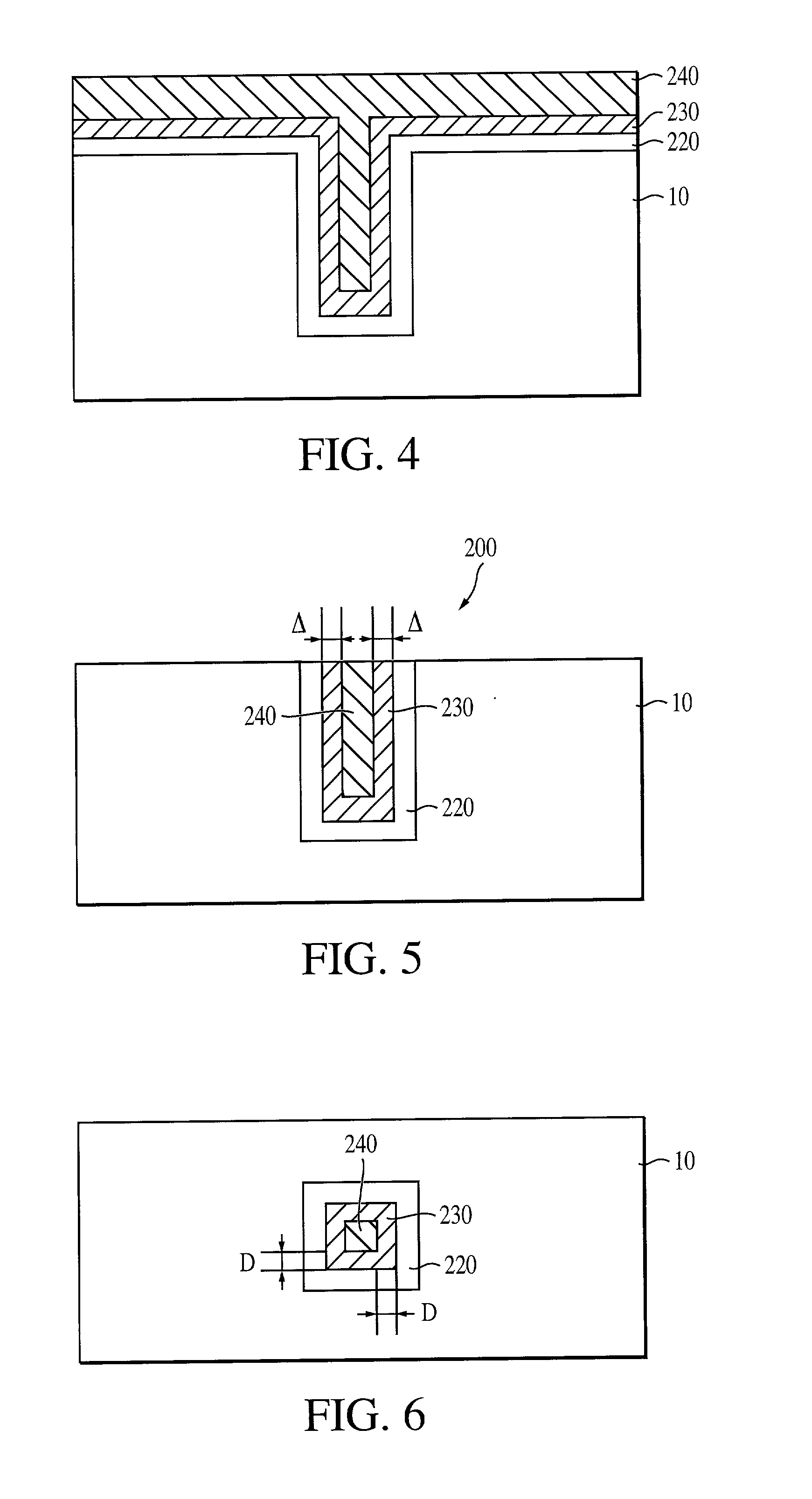
0008] The present invention provides a method of forming an alignment mark for aligning a plurality of empty-spaced patterns formed in semiconductor monocrystalline substrates. According to an exemplary embodiment, alignment metal marks are formed of a conductive material having a melting temperature higher than the annealing temperature used to form the empty-spaced patterns. The alignment marks are formed prior to the formation of empty-spaced buried patterns formed in a monocrystalline substrate, so that the empty-space buried patterns are aligned to the marks. Holes could be next formed in the monocrystalline substrate to connect surfaces of the substrate with the previously formed empty-space patterns. The whole assembly is subsequently exposed to an oxidizing atmosphere so that the inner surfaces of the empty-space patterns are oxidized. The empty-space patterns could then be filled with a suitable conducting material to form, for example, buried conductors and / or buried plate patterns. Subsequent semiconductor structures that are formed as part of desired semiconductor devices can be also aligned to the marks. This way, a proper alignment of the semiconductor devices to the buried conductors and / or buried plate patterns is achieved.

Problems solved by technology

Another problem posed by the formation of the alignment marks under these circumstances is the readability of the mark, particularly when an oxide layer covers the mark.
When the thick oxide layer is later polished, typically by chemical mechanical polishing, to create a planar surface, the alignment marks on a new overlying layer on the wafer are flattened after planarization, causing alignment target reading problems.
Another problem encountered by conventional alignment processes relates to the alignment of various buried structures.
Although the SOI devices have many advantages, such as reduced parasitic capacitance due to the buried insulating layer, the process is relatively expensive because of the high costs of implanting the oxygen atoms and curing of the implant-induced defects.
Further, buried structures such as SOI devices are completely covered by the reformed monocrystalline semiconductor substrate and thus they become essentially non-readable for alignment purposes.

Method used


Image

  • Method of alignment for buried structures formed by surface transformation of empty spaces in solid state materials
  • Method of alignment for buried structures formed by surface transformation of empty spaces in solid state materials
  • Method of alignment for buried structures formed by surface transformation of empty spaces in solid state materials

Examples


Embodiment Construction

[0031] In the following detailed description, reference is made to various exemplary embodiments for carrying out the invention. These embodiments are described with sufficient detail to enable those skilled in the art to practice the invention, and it is to be understood that other embodiments may be employed, and that structural, electrical and process changes may be made, and equivalents substituted, without departing from the invention. Accordingly, the following detailed description is exemplary and the scope of the present invention is defined by the appended claims.

[0032] The term "substrate" used in the following description includes any semiconductor-based structure having an exposed surface in which the structure of this invention may be formed. The term "substrate" is to be understood as including substrates formed of silicon, silicon-on-insulator, doped and undoped semiconductors, epitaxial layers of silicon supported by a base semiconductor foundation, and other semicon...


PUM

PropertyMeasurementUnit
depthaaaaaaaaaa
thicknessaaaaaaaaaa
temperatureaaaaaaaaaa

Abstract

A method of aligning a plurality of empty-spaced buried patterns formed in semiconductor monocrystalline substrates is disclosed. In an exemplary embodiment, high-temperature metal marks are formed to include a conductive material having a melting temperature higher than an annealing temperature used to form such empty-spaced buried patterns. The high-temperature metal marks are formed prior to the formation of the empty-spaced buried patterns formed in a monocrystalline substrate, so that the empty-space buried patterns are aligned to the marks. Subsequent semiconductor structures that are formed as part of desired semiconductor devices can be also aligned to the marks.

Description

[0001] The present invention relates to semiconductor devices and methods of making such devices. More particularly, the invention relates to solid state materials and to a novel method of aligning buried structures formed in such solid state materials.BACKGROUND OF THE IVVENTION[0002] The fabrication of integrated circuits (IC) devices on semiconductor wafers include various steps during which patterns are transferred from photolithographic masks on the wafers. The masking step involves an etching step and defines predefined areas to be exposed on the wafer for subsequent processing, for example, oxidation, metallization, or doping, among others. This photolithographic process is repetitively performed until desired patterns of materials are formed on the semiconductor wafer.[0003] As the dimensions of these patterns become increasingly smaller, it is strictly required to accurately align the patterns previously formed on the semiconductor wafer with a pattern that is to be subsequ...

Claims


Application Information

Patent Timeline
Patent Type & Authority Applications(United States)
IPC IPC(8): G03F9/00H01L21/764H01L23/544
CPCG03F9/7076G03F9/708G03F9/7084H01L21/3247Y10S257/92H01L23/544H01L2223/54453Y10S438/975H01L21/764H01L2924/0002H01L2924/00
Inventor FARRAR, PAUL A.GEUSIC, JOSEPH E.
Owner MICRON TECH INC
Learn More