Semiconductor device with circuitry for efficient information exchange

Inactive Publication Date: 2002-09-12
SOCIONEXT INC
View PDF5 Cites 5 Cited by
  • Summary
  • Abstract
  • Description
  • Claims
  • Application Information

AI Technical Summary

Benefits of technology

[0011] Another and more specific object of the present invention is to provide a semiconductor device which enables efficient data transfer and reduces unnecessary electric power consumption, and to provide a method for making the same.
[0012] In order to achieve the above objects according to the present invention, a semiconductor device, exchanging a data series with an exterior of the device, includes a register which stores a first data item of said data series, the first data item immediately preceding a second data item of said data series, and an exchange circuit which exchanges with the exterior of the device a signal indicative of which bit or bits of the first data item are to be inverted to convert the first data item into the second data item, the exchanging of the signal effectively achieving the exchanging of the data series.

Problems solved by technology

Thus, uncompressed data is redundant and transferring uncompressed data is not efficient.
In some situations, however, it is necessary to transfer uncompressed data between semiconductor devices.
When raw data is transferred without data compression, however, data contains much unnecessary information, and unnecessary electric power is consumed.

Method used


Image

  • Semiconductor device with circuitry for efficient information exchange
  • Semiconductor device with circuitry for efficient information exchange
  • Semiconductor device with circuitry for efficient information exchange

Examples


first embodiment

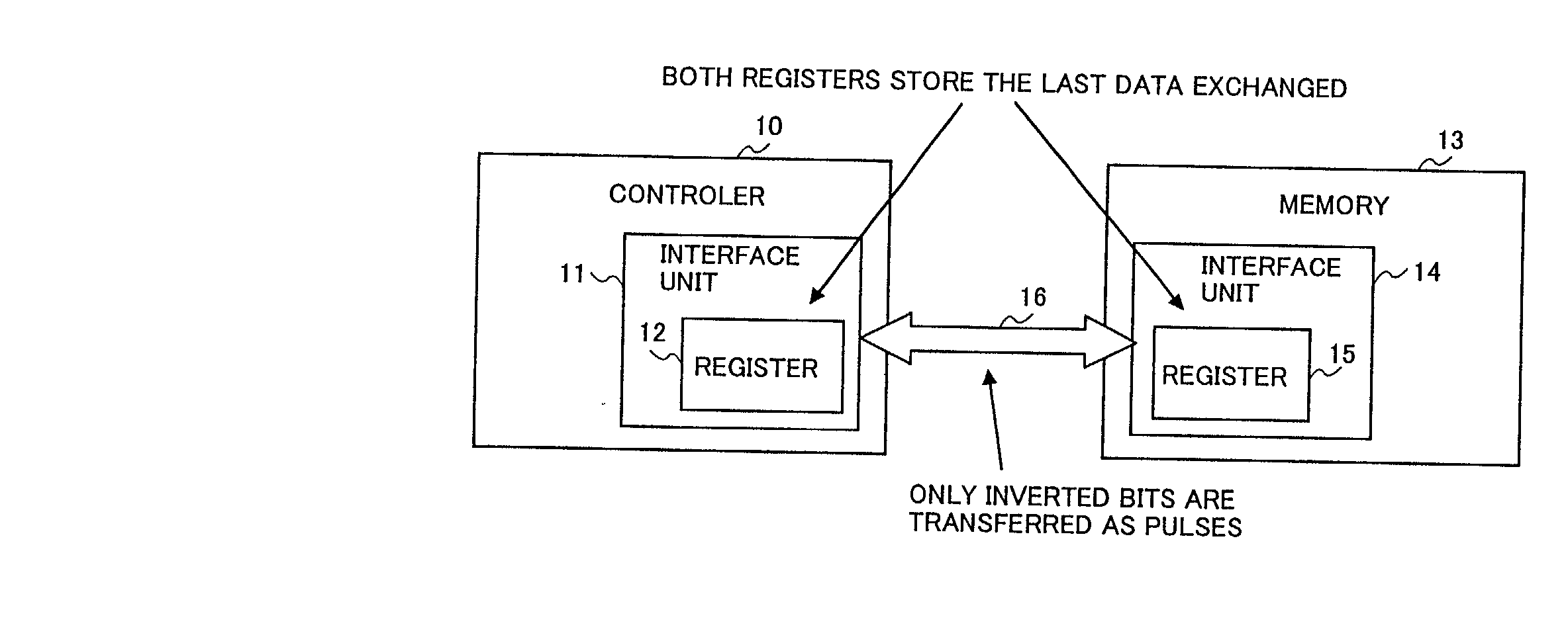
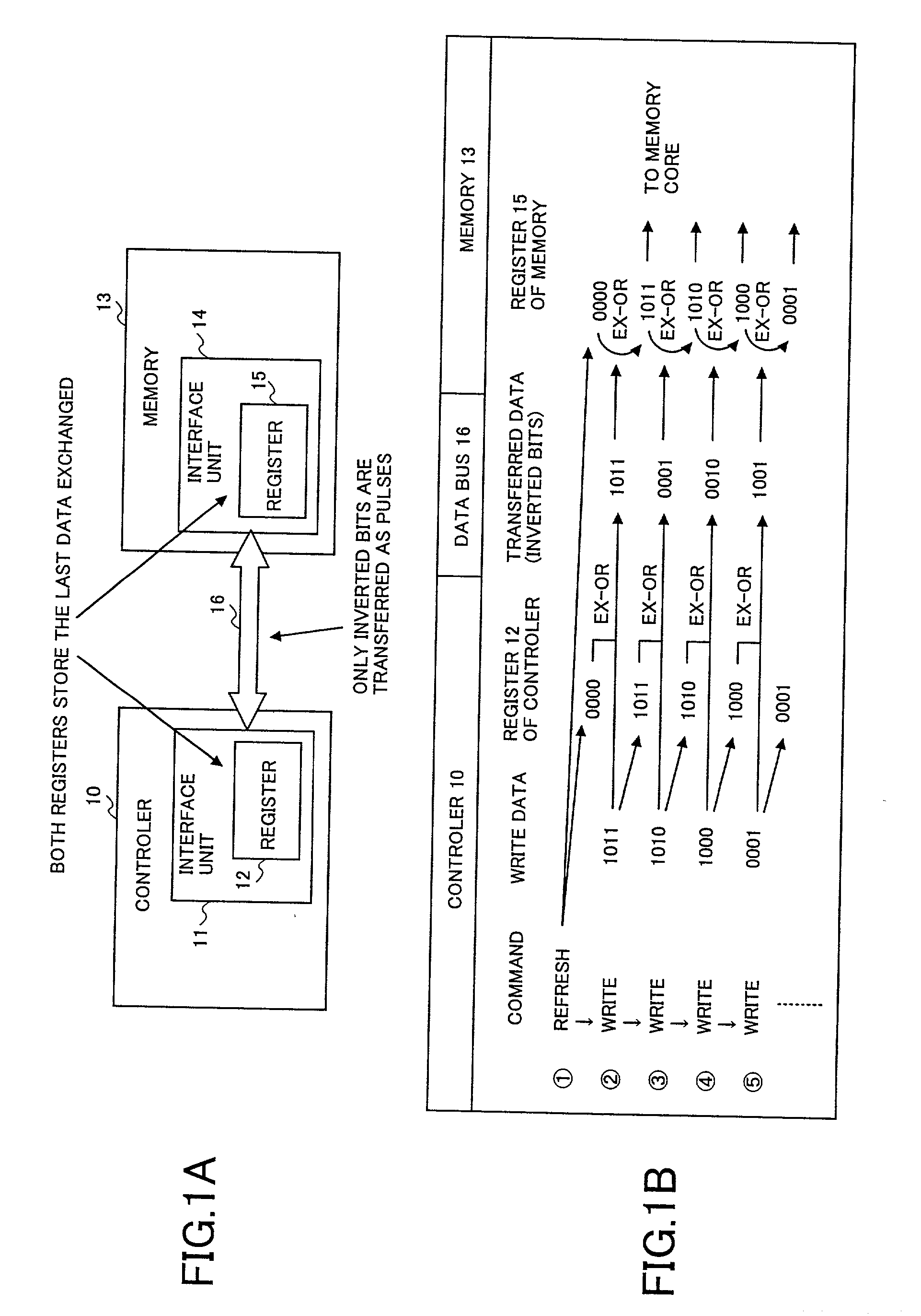
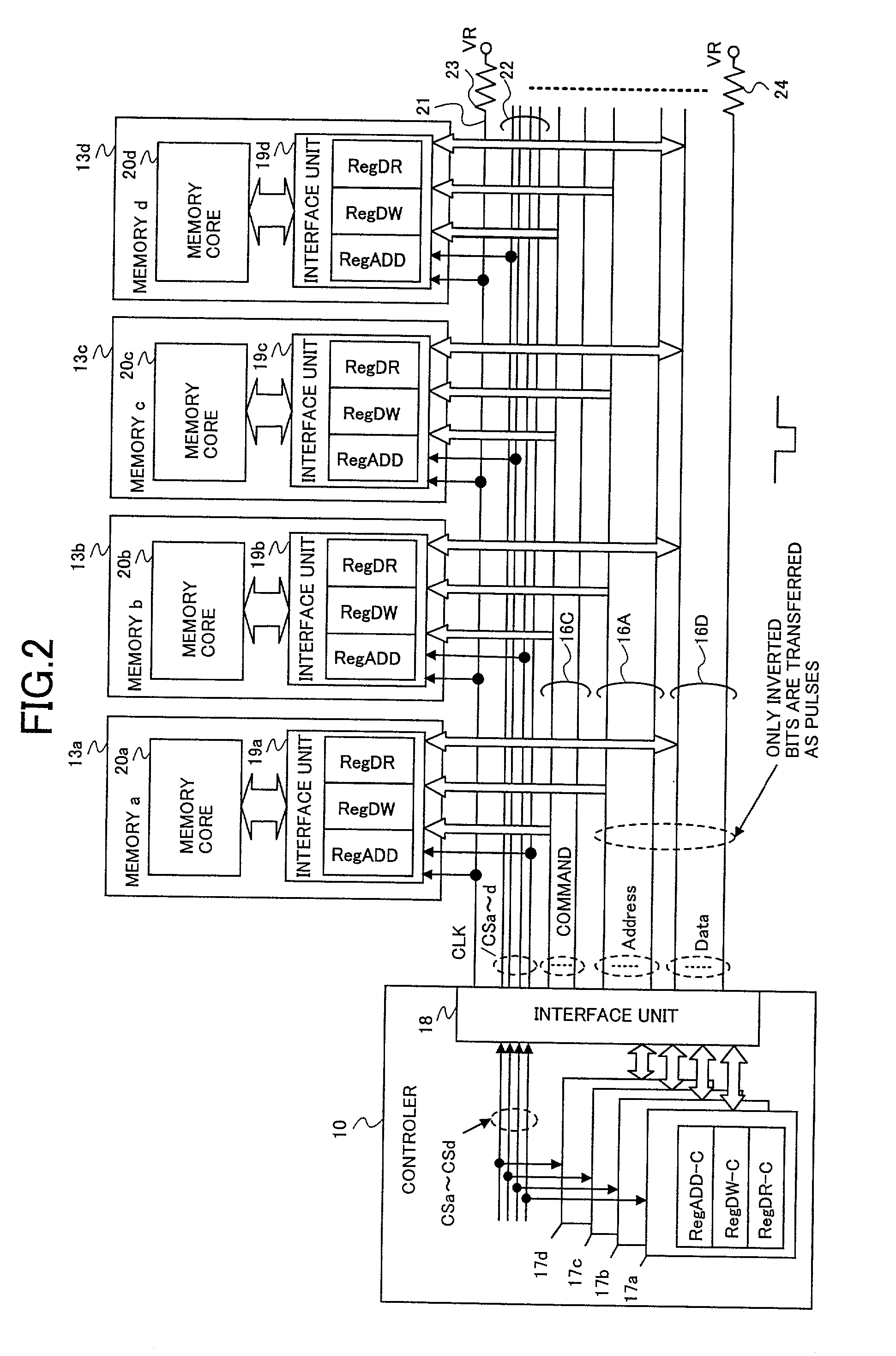
[0081] Each interface unit 19a-19d has a data input unit which receives data (Write Data) from the data bus 16D. FIG. 3 shows the data input unit. The data input unit includes a clock generating unit 25, a command input and decode unit 26, an OR gate 27, and "n" data input units 28.sub.1-28.sub.n where "n" is a natural number. The clock generating unit 25 receives a clock signal from a clock line 21, generates an internal clock CLK1, and sends it to the command input circuit / command decode unit 26 and the data input units 28.sub.1-28.sub.n. The command input circuit / command decode unit 26 is turned ON (Enable mode) when the unit receives a chip select signal CS (any one of CSa-CSd), receives a command through the command bus 16C, and decodes it. The command input circuit / command decode unit 26 drives one of three control lines 33a-33c in accordance with the result of the decoding. In the case of a read command, the command input circuit / command decode unit 26 turns on the control li...

second embodiment

[0095] the data input unit provided in the interface units 19a-19d of the memories 13a-13d will be described below.

[0096] FIG. 6 is a block diagram showing the configuration of the data input unit according to the second embodiment of the present invention. Each unit which is identical to one shown in FIG. 3 is referred to by the same numeral as used in FIG. 3. The second example is a data input unit which is activated by a low-edge, which is an edge observed when voltage goes down to LOW from HIGH.

[0097] Data input units 128.sub.1-128.sub.n are provided instead of the data input units 28.sub.1-28.sub.n shown in FIG. 3. In FIG. 6, however, only the data input unit 128.sub.1 is shown. A 1 / 2 frequency divider 44 is provided. The divider divides an internal clock CLK1 by a ratio of 2, and generates two internal clock signals CLK2 and / CLK2, which are complementary to each other.

[0098] The data input unit 128.sub.1 includes a comparator 29, an inverter 46, an input latch unit 45, a puls...

fifth embodiment

[0116] the data input unit provided in the interfaces 19a-19d of the memories 13a-13d will be described below with reference to FIG. 13. The fifth example is a data input unit which detects LOW edges of the data IN in an asynchronous manner. This is an improvement over the fourth example. Common components to both FIG. 6 and 13 are referred to by the same numerals.

[0117] The circuit of the fifth example is similar to that of FIG. 6, but its input latch unit 62 includes a low-edge detection unit as shown in FIG. 13. This low-edge detection unit includes a gate 47, a comparator 48, a latch 49, and a delay circuit 50. The circuit comprising a gate 51, a comparator 52, and an inverter 63, switches ON and OFF the gate 47.

[0118] FIG. 14 is a timing chart showing the operation of the fifth example described in FIG. 13. An LOW pulse {circumflex over (1)} of the data IN is converted to a HIGH pulse of the data " / IN " by passing through an inverter 46, and is input, through the gate 47, to a ...


PUM


Abstract

A semiconductor device having a register and an information generation circuit can reduce data to be transferred, and consequently save electric power. The register stores first information. The information generation circuit generates, in response to a signal acquired from the an exterior of the device, second information indicating which bits of the first information is to be inverted.

Description

[0001] 1. Field of the Invention[0002] The present invention generally relates to semiconductor devices, and more particularly, to interface method of semiconductor devices.[0003] 2. Description of the Related Art[0004] It is necessary, in some cases, to transfer data between semiconductor devices. The following case of transferring two sets of 16 bit width data, D1 and D2, sequentially from a semiconductor device A to another semiconductor device B, will be considered as an example.[0005] D1:1100110011001100[0006] D2:1100110011001101[0007] In this case, only the last bit is different from each other, and the other bits are the same. Generally, in case of sequential data of moving pictures for example, data is almost the same as the next data, and only a part of data is different. Thus, uncompressed data is redundant and transferring uncompressed data is not efficient. Data is usually compressed, then transferred or stored into recording medium.[0008] In some situations, however, it...

Claims


Application Information

Patent Timeline
IPC IPC(8): G11C7/10H03M5/14G06F12/02H03M7/00H03M7/30
CPCG11C8/10H03M5/14H03M7/00H03M7/30G11C7/10
Inventor MATSUZAKI, YASUROUTAGUCHI, MASAO
Owner SOCIONEXT INC
Why Eureka
Try Eureka