Evaluating a multi-layered structure for voids

a multi-layered structure and void technology, applied in the direction of optical radiation measurement, semiconductor/solid-state device testing/measurement, instruments, etc., can solve the problems of void formation, void formation, void formation, etc., and achieve the effect of reducing or eliminating voids

Inactive Publication Date: 2002-09-12
APPLIED MATERIALS INC
View PDF0 Cites 22 Cited by
  • Summary
  • Abstract
  • Description
  • Claims
  • Application Information

AI Technical Summary

Benefits of technology

0016] A method and apparatus in accordance with the invention measure properties of two layers of a damascene structure (e.g. a silicon wafer during fabrication), while scanning, and use the two scanning measurements to identify a location as having voids. The two scanning measurements can be used in any manner, although in one embodiment, the two measurements are compared to one another (either automatically by computer during the scanning or visually by an operator after the scanning). Voids are dee...

Problems solved by technology

If the sidewall coverage is too thin, then the coating may be discontinuous, or even non-existent.
It then acts as a poor nucleating surface for the subsequent electrodeposition of subsequent thick layer 106, causing problems such as void formation.
Specifically, voids may arise if the plating process does not begin properly on one of the sidewalls.
For example, filling may not start at the bottom of a groove, resulting in a "bottom" void.
If the coating is too thick, the top of the groove may close off, preventing adequate circulation of electrodeposition electrolyte, resulting in poor filling of the grooves which can also result in voids.
Also, voids may be created between a metal line and the underlying dielectric layer due to volume contraction that occurs after annealing.
Furthermore, stress- and electromigration voids typically nucleate at intersections of metallization grain boundaries and the passivation/interconnect interface, and can form as a consequence of current flowing through...

Method used


Image

  • Evaluating a multi-layered structure for voids
  • Evaluating a multi-layered structure for voids
  • Evaluating a multi-layered structure for voids

Examples


Embodiment Construction

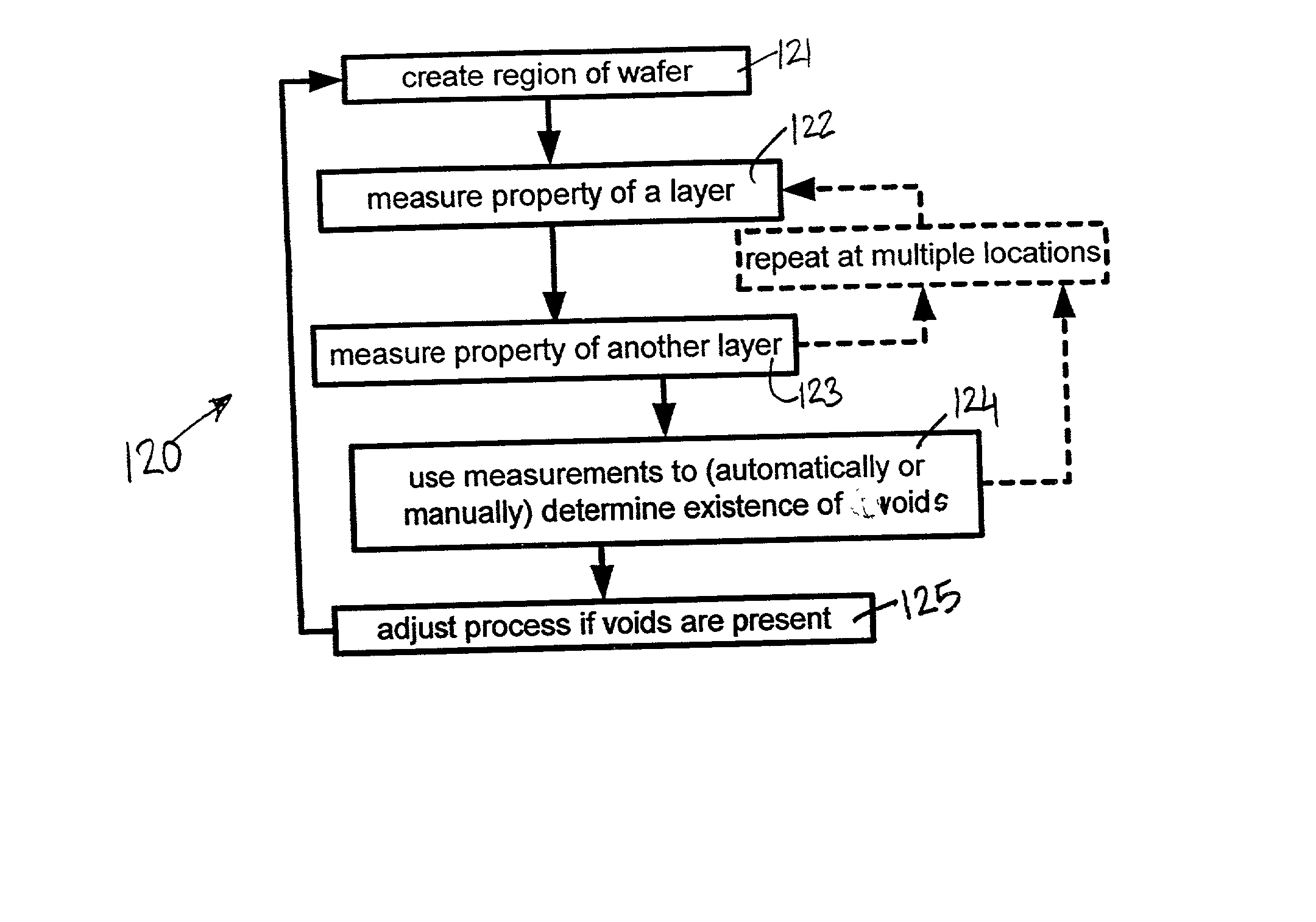
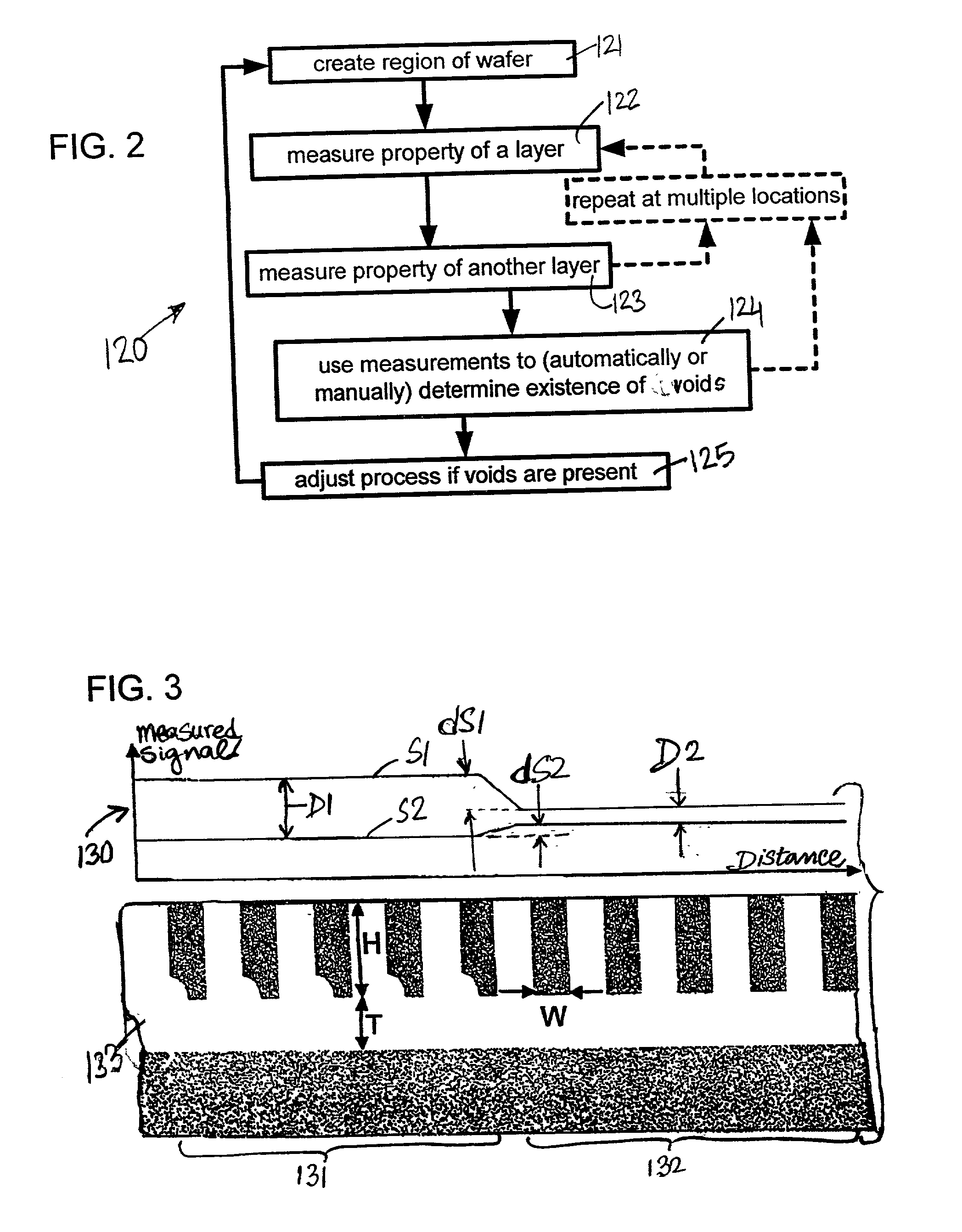
[0036] One embodiment measures (e.g. see acts 122 and 123 in FIG. 2) properties of two layers of a structure, and uses the two measured signals to determine existence of voids (see act 124). Measurements (as illustrated by signals S1 and S2 in FIG. 3) change depending on the presence and absence of voids (see the change in signals S1 and S2 in regions 131 and 132 respectively) when a scan is performed across a wafer. In the example illustrated in FIG. 3, signal S1 reduces by the amount dS1 and signal S2 increases by an amount dS2, so that a separation D1 between S1 and S2 in the presence of voids is reduced to the separation D2.

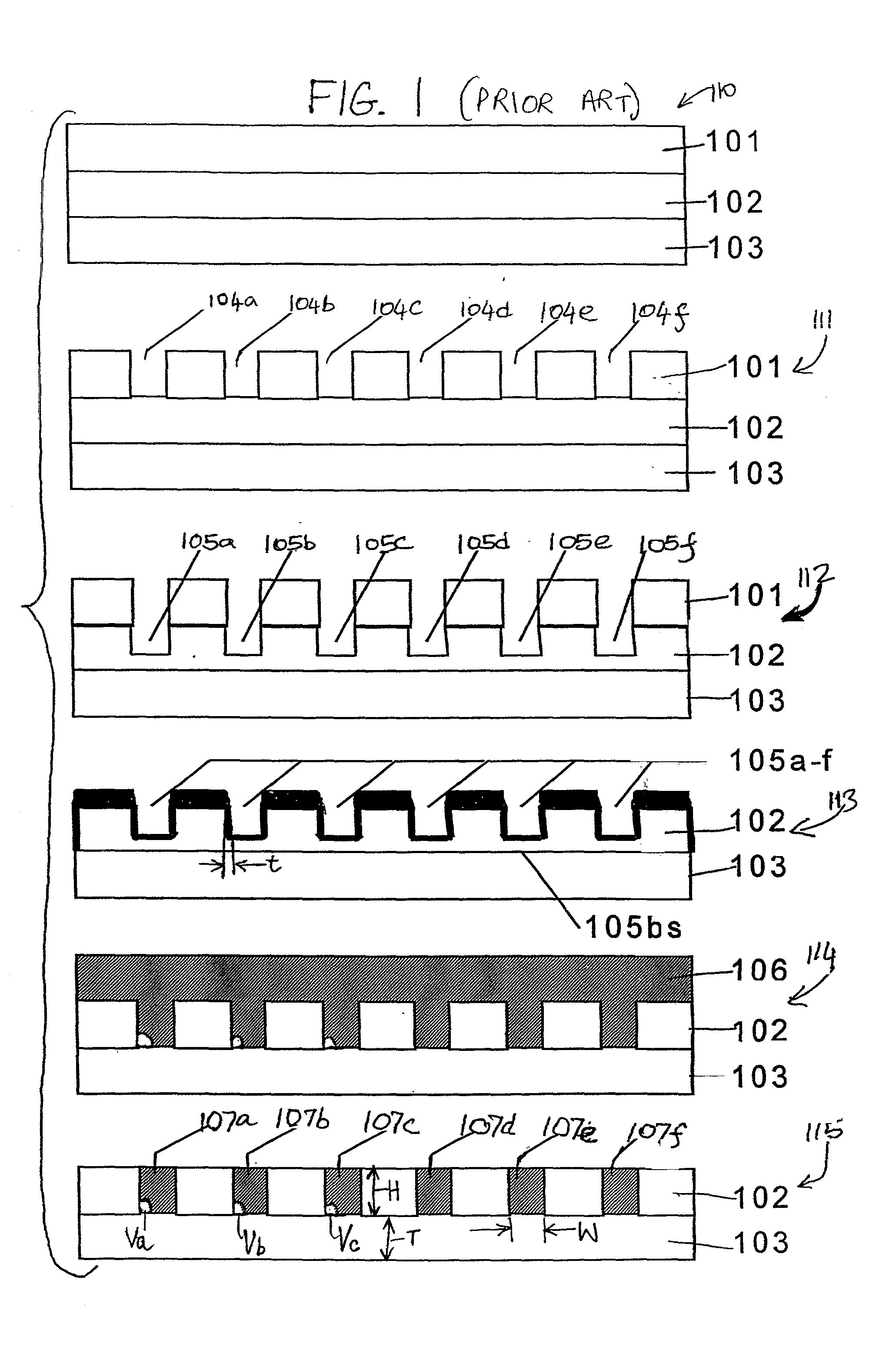
[0037] The above-described acts 122-124 for finding voids are effective even in a damascene structure that is formed in the normal manner, e.g. by etching grooves in a dielectric layer and forming conductive traces (also called "lines") inside the grooves as illustrated in FIG. 1. During fabrication of the damascene structure, voids can be formed between the ...


PUM


Abstract

A method and apparatus measure properties of two layers of a damascene structure (e.g. a silicon wafer during fabrication), and use the two measurements to identify a location as having voids. The two measurements may be used in any manner, e.g. compared to one another, and voids are deemed to be present when the two measurements diverge from each other. In response to the detection of voids, a process parameter used in fabrication of the damascene structure may be changed, to reduce or eliminate voids in to-be-formed structures.

Description

CROSS-REFERENCE TO RELATED APPLICATIONS[0001] This application is related to and incorporates by reference herein in their entirety the following commonly owned U.S. patent applications:[0002] Ser. No. 09 / 095,805 entitled "AN APPARATUS AND METHOD FOR MEASURING A PROPERTY OF A LAYER IN A MULTILAYERED STRUCTURE", filed Jun. 10, 1998 by Peter G. Borden et al. which is now issued as U.S. Pat. No. 6,054,868;[0003] Ser. No. 09 / 521,232 entitled "EVALUATING A PROPERTY OF A MULTILAYERED STRUCTURE", filed on Mar. 8, 2000 by Peter G. Borden et al.;[0004] Ser. No. 09 / 544,280 entitled "AN APPARATUS AND METHOD FOR EVALUATING A WAFER OF SEMICONDUCTOR MATERIAL", filed Apr. 6, 2000 by Peter G. Borden et al., which is a continuation of Ser. No. 09 / 095,804 filed Jun. 10, 1998 and now issued as U.S. Pat. No. 6,049,220; and[0005] Attorney Docket No. M-12169 US, entitled "IDENTIFYING DEFECTS IN VIAS OF A WAFER, BASED ON HEAT TRANSFER THERETHROUGH" filed concurrently herewith, by Peter G. Borden and Ji-Pi...

Claims


Application Information

Patent Timeline
IPC IPC(8): G01DG01N21/00G01N21/17G01N21/21G01N21/84G01N21/88G01N21/95G01R31/26G01R31/265H01L21/265H01L21/4763H01L21/66
CPCG01N21/171G01N21/1717G01N21/21G01N21/211G01N21/8422G01N21/9501G01N21/9505G01N21/95607G01N21/95692G01N2021/1748G01N2021/216G01R31/2648G01R31/2656H01L22/12
Inventor BORDEN, PETER G.LI, JI-PING
Owner APPLIED MATERIALS INC
Why Eureka
Try Eureka