

Pll cycle slip compensation
- Summary
- Abstract
- Description
- Claims
- Application Information
AI Technical Summary
Benefits of technology
Problems solved by technology
Method used
Image

Examples
Embodiment Construction
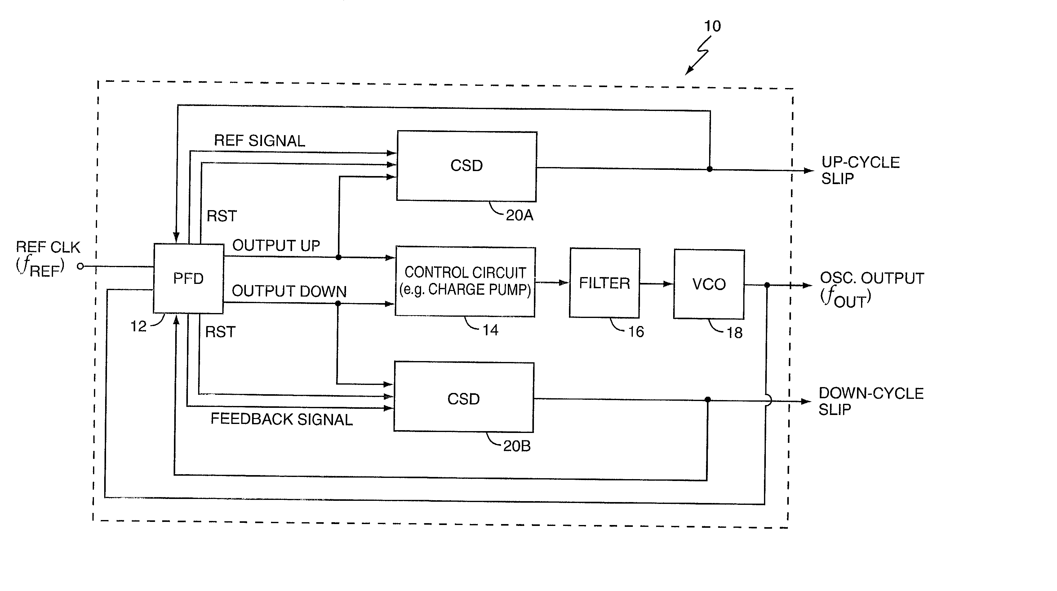
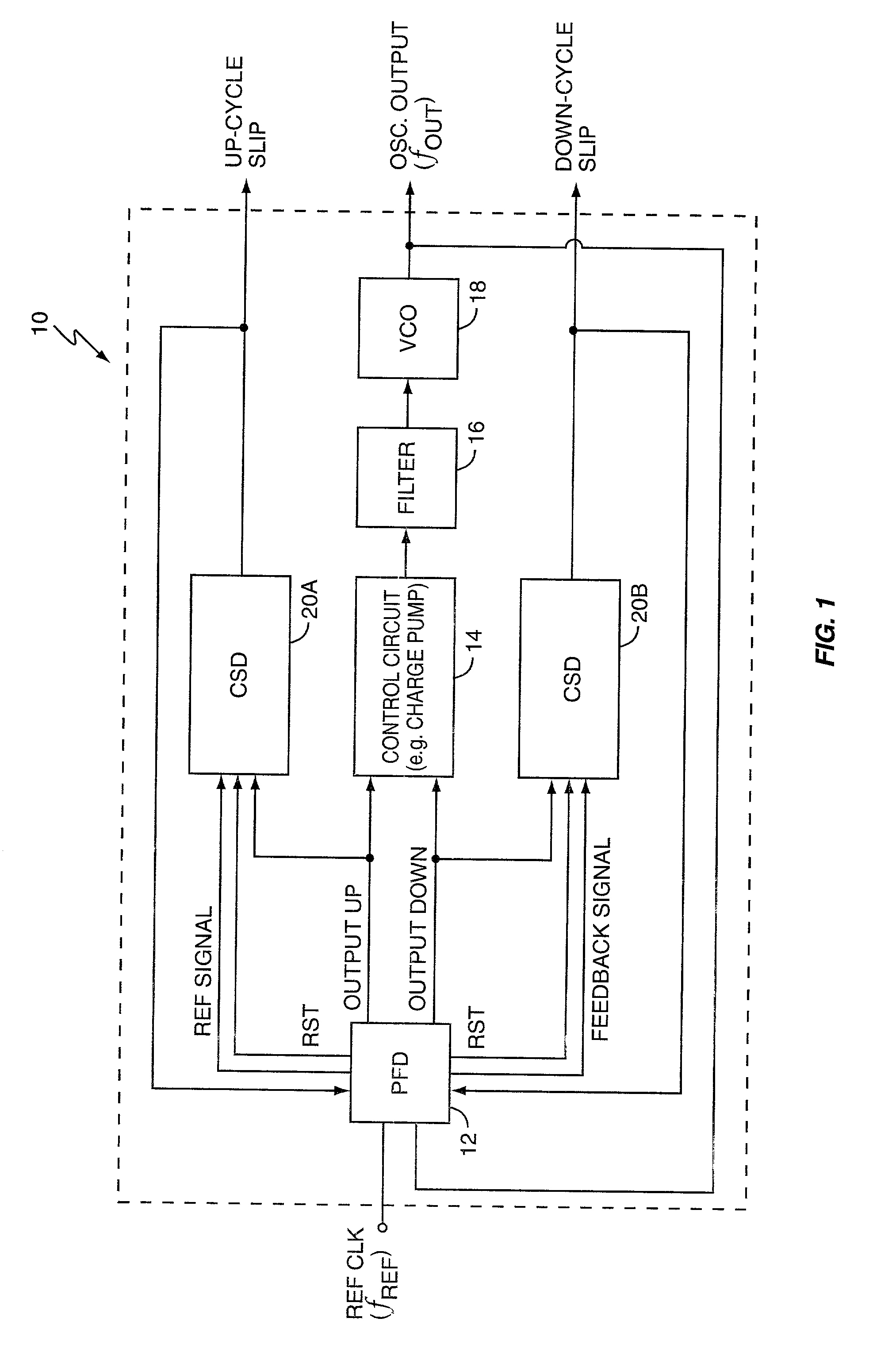
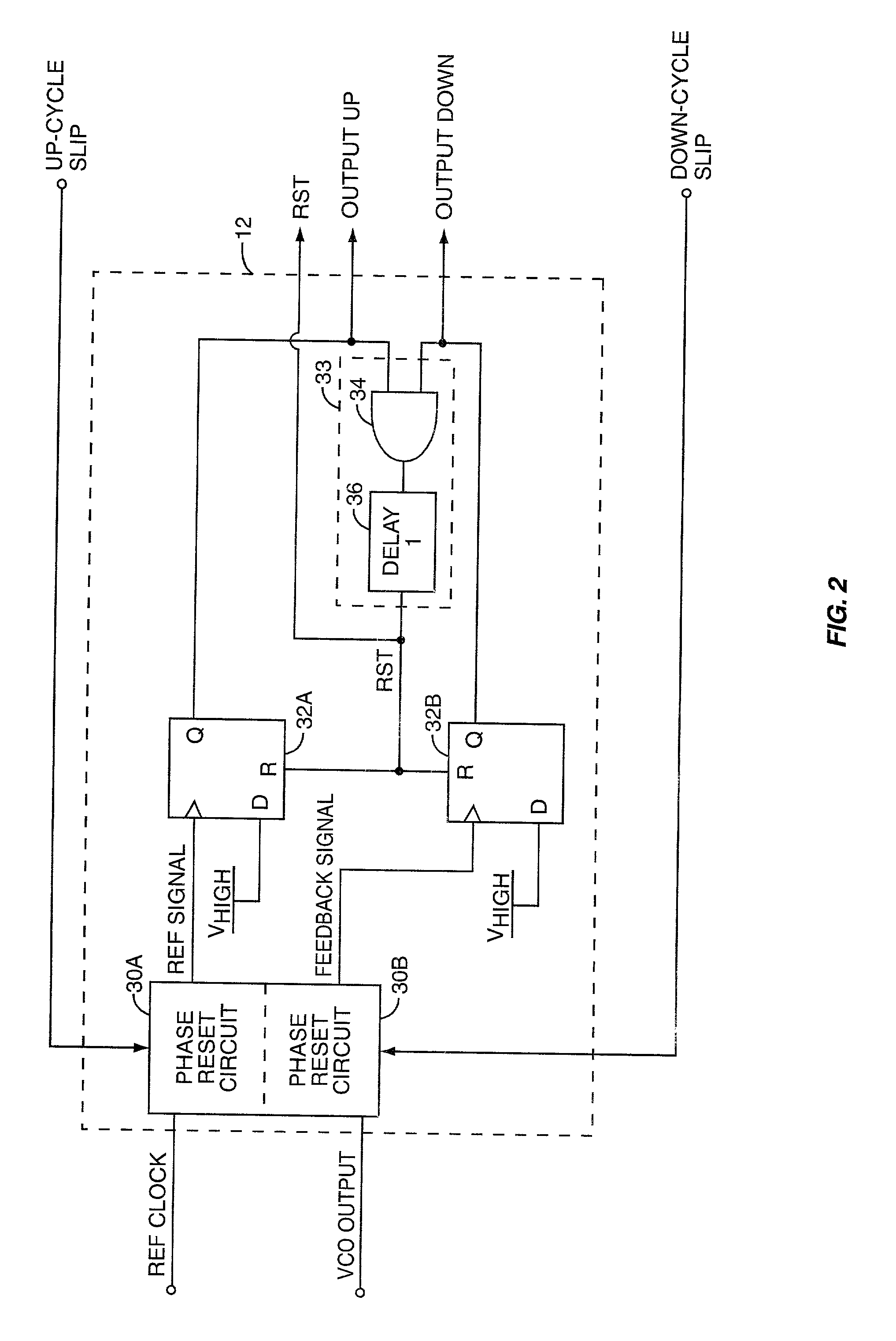
[0012] Turning now to the drawings, FIG. 1 is a diagram of a PLL, generally referred to by the numeral 10. The PLL 10 comprises a phase / frequency detector (PFD) 12, a control circuit 14, a loop filter 16, a voltage-controlled oscillator (VCO) 18, and cycle slip detectors 20A and 20B.
[0013] The PFD 12 receives two input signals, a reference clock signal and the output signal from the VCO 18. The output signal from the VCO 18 is made to have a frequency that is a desired multiple or fraction of the reference clock frequency by operation of the PLL 10. The PFD 12 typically generates two output signals, OUTPUT UP and OUTPUT DOWN, to control the control circuit 14. The PFD 12 controls the control circuit 14 via the OUTPUT UP / DOWN signals to adjust the control voltage applied to the VCO 18. The loop filter 16 translates the output from the control circuit 14 into a smoothed, voltage-mode control signal for the VCO 18. In this manner, the frequency of the output signal from the VCO 18 is l...
PUM
 Abstract
Description
Claims
Application Information